Lab 0 — Introduction to XSchem and Magic
ECE334 — Digital Electronics — SKY130 open-source flow
Objective
Get the toolchain working and build something with it. There are no marks for this lab. Do it anyway: every later lab assumes you can place a symbol, wire a schematic, run a simulation, and open a layout without being told how.
By the end you will have:
- drawn a CMOS inverter from individual transistors and simulated it;
- turned it into a reusable symbol, and built a 2-input NAND the same way;
- wired both into a pulse generator and seen what it does;
- painted a transistor in Magic; and
- worked through
lab0.ipynb, which is where you learn the notebook that Labs 1 to 4 are reported in.
Keep the XSchem and Magic cheatsheets open in another tab.
The tools
| File | Purpose |
|---|---|
lab0.ipynb |
The notebook tutorial. Self-contained: it runs against a deck that ships with the lab, so it works before your schematic does. |
spice/inv_demo.spice |
A CMOS inverter as a plain deck. Read it — every testbench in this course has the same five parts. |
xschem/, magic/ |
Empty. This is the lab where you fill them. |
Course conventions
| Setting | Value |
|---|---|
| Process (PDK) | sky130A |
| Supply voltage | 1.8 V |
| Teaching channel length | L = 0.5 µm |
| NMOS / PMOS devices | sky130_fd_pr__nfet_01v8 / sky130_fd_pr__pfet_01v8 |
| Unit inverter | Wn = 1, Wp = 3 |
| NAND2 | Wn = 2 (series pair), Wp = 3 (parallel pair) |
| Extraction device (Lab 1 P2) | W = 10, L = 2 |
Widths and lengths are entered as unitless microns: W=1, L=0.5. A u
suffix means metres, lands outside every model bin, and makes ngspice report
"could not find a valid modelname".
Preparation
Set up the environment first — see Getting started. Then, in the desktop terminal:
.designinit loads the SKY130 technology and installs the course XSchem
configuration. Source it once per terminal. If a tool behaves oddly later, run
it again — it is idempotent and fixes most configuration problems.
Work in lab0_setup. That folder is mounted from your own clone, so anything
you save there survives restarting the container.
Watch the terminal you launched from. XSchem and Magic print their warnings and errors there, not in the GUI.
L1 — XSchem
L1.1 Getting around
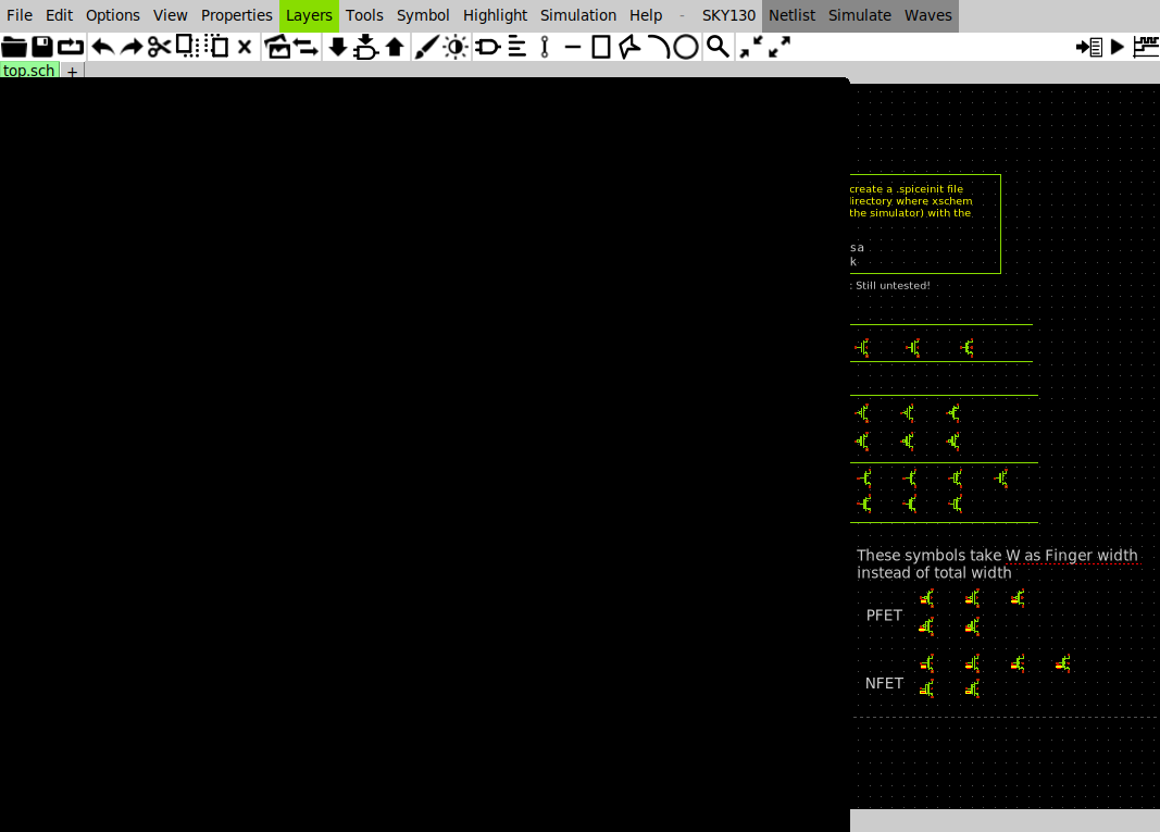 Menu bar, toolbar, and drawing canvas. Messages appear at the bottom and in the
terminal.
Menu bar, toolbar, and drawing canvas. Messages appear at the bottom and in the
terminal.
| Action | Key |
|---|---|
| Zoom to fit | f |
| Zoom in / out | Shift-Z / Ctrl-Z, or scroll |
| Pan | hold Space and drag |
| Keybinding overlay | ? |
| Abort whatever you started | Ctrl-C |
Spend a minute panning and zooming an empty canvas before placing anything.
L1.2 Placing transistors
Press Shift-I to open the symbol browser, or use Tools → Insert symbol.
Navigate to the SKY130 device library and place:
sky130_fd_pr/nfet_01v8.symsky130_fd_pr/pfet_01v8.sym
Select each device and press q to edit its properties.
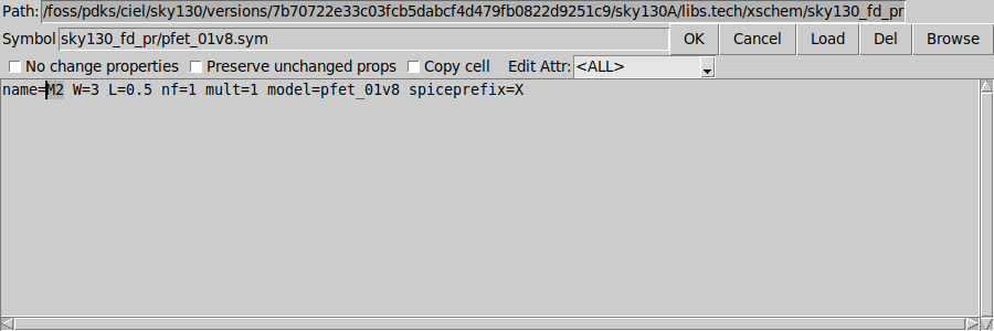 Set
Set W and L only. spiceprefix, nf and the diffusion geometry come from
the symbol.
Set W=1 L=0.5 on the NMOS and W=3 L=0.5 on the PMOS.
No u on W or L
W=1, not W=1u. The SKY130 models are binned on plain micron numbers. A
value in metres falls outside every bin and ngspice stops with "could not
find a valid modelname". Expect to hit this at least once.
L1.3 Wiring the inverter
Press w to draw wires. Click to start and to turn a corner; middle-click to
finish. Connect:
- PMOS: source to
vdd, drain toout, gate toin, body tovdd - NMOS: source to
vss, drain toout, gate toin, body tovss
Add ports from the devices library: ipin for in, opin for out, and
iopin for vdd and vss.
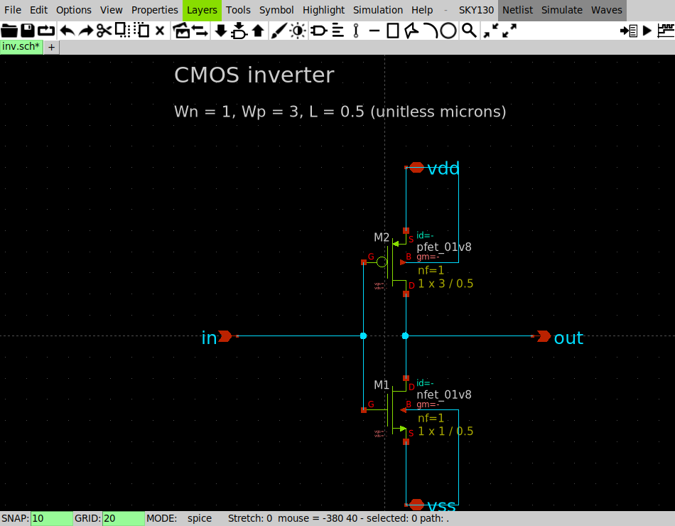 The finished cell. The device symbols are drawn source-outward, so the PMOS
source already faces
The finished cell. The device symbols are drawn source-outward, so the PMOS
source already faces vdd with no flipping.
A hollow square on a port means it is not connected. Crossing wires do not connect; only a wire endpoint landing on another wire or a port does. Zoom in and check every square before moving on.
Save with Ctrl-S as inv.sch.
L1.4 Making a symbol
Symbol → Make symbol from schematic (A) generates a symbol from the ports,
then c swaps between the schematic and symbol views. Shift-C is draw arc,
not make-symbol — press it by mistake and you leave a stray arc behind.
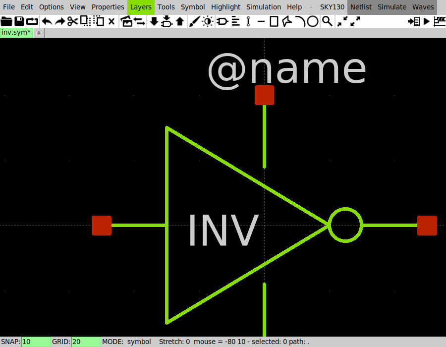 Symbol view. Red squares are the pins.
 @name is substituted with each
instance's name when the symbol is placed.
This is what hierarchy means here: inv.sym is now a part you can place in
another schematic, and XSchem pulls in inv.sch when it netlists.
Compare yours against common/xschem/inv.sym, which the later labs use.
L1.5 A 2-input NAND
Build nand2.sch the same way: two PMOS in parallel from vdd to out, two
NMOS in series from out to vss. Use W=2 for the series NMOS pair and
W=3 for the PMOS.
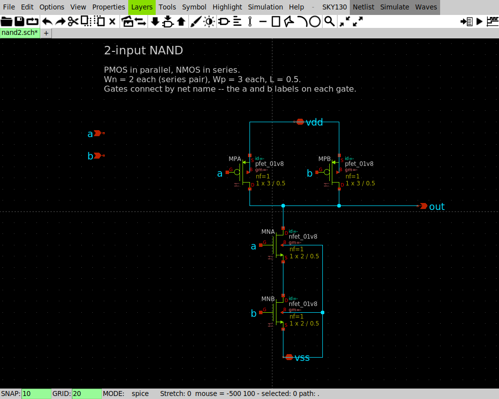 Parallel PMOS on top, series NMOS below. Gates connect by net name — the
 a
and b labels — which keeps the drawing readable.
The series pair is doubled in width because two devices in series behave like one device of half the width. Convince yourself of that before Lab 3, where you size a more complicated gate the same way.
Make a symbol for it too.
L1.6 A pulse generator
Now use both cells. Wire three inverters in a chain, feed the chain output to
one NAND input and the original signal to the other, and drive the whole thing
with a pulse source.
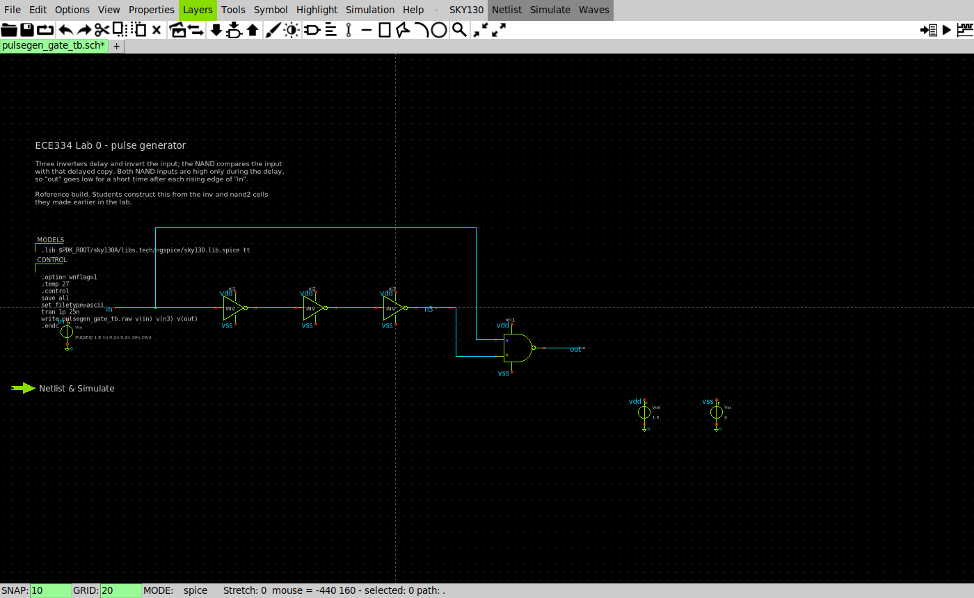 Three
Three inv instances and one nand2, with the input tapped along the top to
the NAND's other pin. Supplies connect by name through vdd and vss labels.
Add a code_shown block with the model include and a .control block, then
click Netlist then Simulate in the menubar:
Plot with the menubar: Waves → Tran, then pick the .raw the simulation
wrote. (p is draw polygon in XSchem, not plot.)
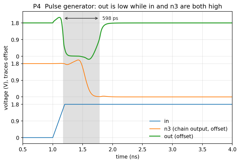 Each rising edge of
 in produces one short low-going pulse on out.
Look at what happened. in goes high. The chain output n3 stays high for a
while, because each inverter takes time to switch. During that window both NAND
inputs are high, so out goes low. When n3 finally falls, out returns high.
The pulse is therefore as wide as the inverter chain is slow. You are not asked to predict that width here — Lab 1 builds the model for it, starting from an RC circuit and ending at exactly this measurement. For now, note the width you observe, and note that it changes if you change the number of inverters.
L2 — Magic
Layout is where the circuit becomes geometry. Lab 2 does a full cell; here you only draw one transistor.
cd /foss/designs/lab0_setup/magic
echo "source \$PDK_ROOT/sky130A/libs.tech/magic/sky130A.magicrc" > .magicrc
magic -d X11 -T sky130A fet &
Magic opens a layout window and a tkcon console. Commands go in tkcon.
L2.1 The box
Magic acts on the box, a rectangle you position first. Left-click one corner, right-click the other. Or set it exactly:
L2.2 Painting a transistor
Paint a strip of diffusion, then cross it with poly:
Add a contact at each end so the source and drain can be wired. Paint the local interconnect first, then the contact inset inside it:
box 0.05um 0.1um 0.55um 0.9um
paint li
box 0.15um 0.2um 0.45um 0.8um
paint ndcontact
box 1.25um 0.1um 1.75um 0.9um
paint li
box 1.35um 0.2um 1.65um 0.8um
paint ndcontact
A contact with no li over it fails DRC everywhere
Rule li.5 wants local interconnect overhanging every cut. Paint the two
ndcontact rectangles on their own and Magic reports 16 violations, not
zero — which is why the li rectangle comes first and the contact is inset
inside it. You meet the same rule again in Lab 2, on every contact in the
NAND2.
Press v to fit the view.
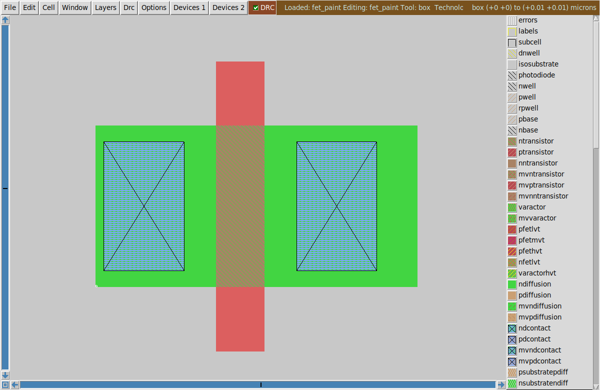 Green
Green ndiffusion crossed by red poly, with a diffusion contact at each end.
The layer palette is on the right; the DRC status is in the toolbar.
You never placed a transistor. Magic infers one from the overlap: poly over diffusion is a gate, and the diffusion either side becomes source and drain. Check it:
L2.3 Design rules
Magic checks design rules continuously. Violations appear as white dots and a count in the toolbar. Try it: move the poly to within a hair of a contact and watch the dots appear.
drc why names the rule that was broken, which is faster than guessing. Get
back to zero before you finish.
Save by typing save fet in tkcon, or File → Save. Magic binds Ctrl-S to
select less, so it writes nothing and gives no warning.
L3 — The notebook
Labs 1 to 4 are reported through a Jupyter notebook, and none of them stop to explain it. This is where you learn it, with a demonstrator in the room.
Open lab0.ipynb and work through it. It covers running a cell, why order
matters, loading a simulation result, measuring it, plotting it, and the
hand-analysis → measurement → written-answer shape every later section uses. It
also makes you cause a few of the common errors on purpose, so you recognise
them later.
Finish with Kernel → Restart Kernel and Run All Cells. That habit is worth forming now: it is the only way to know your notebook runs top to bottom on someone else's machine, which is how it will be marked.
Expected results
Nothing is submitted. Before Lab 1, confirm you can:
- [ ] place a transistor and set
WandLwithout theuerror; - [ ] wire a schematic with no unconnected ports left;
- [ ] make a symbol and instantiate it in another schematic;
- [ ] run a simulation and plot a net;
- [ ] paint geometry in Magic and reach
drc count= 0; and - [ ] run
lab0.ipynbend to end from a restarted kernel with no errors.
Extra notes
.designinitis idempotent. Re-run it whenever something stops resolving.- XSchem writes results to
/foss/designs/.xschem/simulations. - Keys that differ from most editors: in XSchem
ccopies andqopens properties; in Magicddeletes andsselects. - Names are one flat namespace across labs. If you invent a cell name that a later lab also uses, one will shadow the other. Prefix yours if unsure.
FAQ
The symbol browser opens in the wrong folder. Click Home to return to the top of the tree, then navigate again.
I placed a transistor but the netlist has no devices.
Either the DUT or schematic was never saved, or XSchem cannot resolve the
symbol. Re-run .designinit and reopen.
Magic says Failed to load technology.
No .magicrc in the directory you started from. Create it as shown above.
My layout window is blank except for one labelled rectangle.
That is an unexpanded subcell. Press x.