Lab 2 — NAND gate layout, DRC, LVS and extraction
ECE334 — Digital Electronics — SKY130 open-source flow
Objective
Draw the physical layout of the 2-input NAND you built in Lab 1, prove it is manufacturable, prove it is the circuit you meant to draw, and then measure what the physical implementation costs you in speed.
Four checks, in order, each of which can fail independently:
| Check | Question it answers | Tool |
|---|---|---|
| DRC | Can this be manufactured? | Magic |
| Extraction | What circuit did I actually draw? | Magic |
| LVS | Is that the circuit I intended? | Netgen |
| PEX | What does the physical wiring cost? | Magic + ngspice |
A layout that passes DRC can still be the wrong circuit. A layout that passes LVS can still be slow. You need all four.
Course conventions
| Setting | Value |
|---|---|
| Process (PDK) | sky130A |
| Supply voltage | 1.8 V |
| Teaching channel length | L = 0.5 µm |
| NMOS / PMOS devices | sky130_fd_pr__nfet_01v8 / sky130_fd_pr__pfet_01v8 |
| Unit inverter | Wn = 1, Wp = 3 |
| NAND2 | Wn = 2 (series pair), Wp = 3 (parallel pair) |
| Extraction device (Lab 1 P2) | W = 10, L = 2 |
Widths and lengths are entered as unitless microns: W=1, L=0.5. A u
suffix means metres, lands outside every model bin, and makes ngspice report
"could not find a valid modelname".
The tools
| File | Purpose |
|---|---|
magic/ |
Where you draw the layout. Magic writes nand2.mag here. |
xschem/nand2_lvs.sch |
Wrapper that instantiates nand2.sym, so XSchem emits a .subckt for netgen to compare against. |
lab2.ipynb |
Your report. Captures the DRC count, the extracted netlist, the LVS verdict, and the delay comparison. |
spice/nand2_compare.spice |
The L6 testbench. Runs against either extracted netlist by swapping one .include. |
Lab 2 produces mostly tool output rather than waveforms, so the notebook captures that output rather than re-deriving it. Run its cells after you have finished in Magic.
The cell is the Lab 1 NAND2: Wn = 2 (series pair), Wp = 3 (parallel pair),
L = 0.5. Those are the legacy handout's \((W/L)_p = 24\), \((W/L)_n = 16\) ratios
at this lab's channel length. Ports: a, b, out, vdd, vss — the same
names as common/xschem/nand2.sch, so LVS compares like with like.
Preparation
P1 — Read the Magic tutorial
Work through the MAX/Magic tutorial on Quercus before the session. The Magic cheatsheet is the short version.
P2 — Draw a stick diagram
On paper, with coloured pens, sketch the NAND2 as a stick diagram. Do not use metal2 and do not worry about exact dimensions. Decide, before you touch the tool:
- which diffusion strip is NMOS and which is PMOS;
- where each poly gate crosses;
- which diffusion regions are shared, and which need a contact;
- where the two supply rails run, and where the well and substrate taps go.
The series NMOS pair shares its middle diffusion region with no contact at all. Convince yourself that is legal before you draw it.
P3 — Predict the parasitics
The layout adds capacitance the schematic does not have: diffusion to substrate, poly to substrate, and interconnect to everything nearby. Before L6, write down whether you expect that to matter more when the gate drives a large load or a small one, and why.
Lab Work
L1 — Set up
. /foss/designs/common/.designinit
cd /foss/designs/lab2_layout
echo "source \$PDK_ROOT/sky130A/libs.tech/magic/sky130A.magicrc" > .magicrc
magic -d X11 -T sky130A nand2 &
Use the X11 driver. Magic opens two windows: the layout, and tkcon, where you type commands.
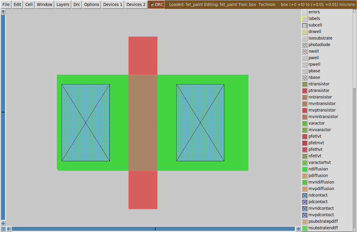 The layout window, with the layer palette on the right and the live DRC status
in the toolbar.
The layout window, with the layer palette on the right and the live DRC status
in the toolbar.
L2 — Draw the layout
Build the cell. Horizontal diffusion, vertical poly:
- NMOS,
ndiff, 2 µm tall, with two poly stripes crossing it. The regions are: source (tovss), the shared middle node, and drain (toout). - PMOS,
pdiff, 3 µm tall, inside annwell, with the same two poly stripes. Regions: source, shared drain (out), source. - Contacts
ndcandpdcon every region that leaves the device — not on the NMOS middle node. - Taps:
ptap/ptapctied tovss,ntap/ntapcinside the nwell tied tovdd. A layout without taps will extract, and will not work. - Rails in
met1, connected down toliwithmcon.
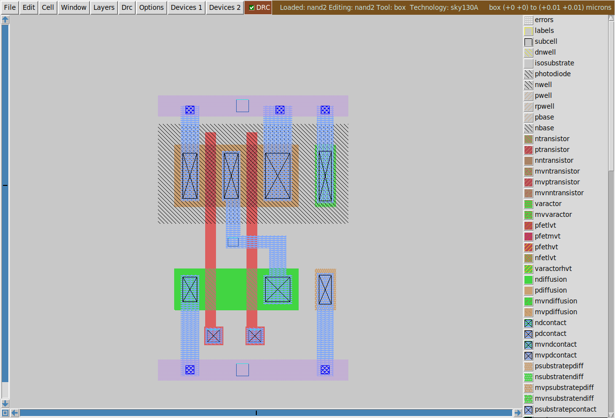 Reference layout. PMOS pair in the nwell (top), series NMOS below, two poly
gates crossing both,
Reference layout. PMOS pair in the nwell (top), series NMOS below, two poly
gates crossing both, li routing in blue, met1 rails top and bottom, and the
two taps at the right.
Contacts need local interconnect around them
Paint li over a slightly larger rectangle than the contact itself. The cut
needs at least 0.08 µm of li overhanging it (rule li.5), and a contact
painted with no surrounding li fails DRC everywhere it appears. Painting
li first and then the contact inset by 0.1 µm satisfies the rule
everywhere without measuring each cut.
Label every port: place the box over the shape and type label a, and so on for
b, out, vdd, vss.
L3 — DRC to zero
DRC runs continuously; violations appear as white dots with a live count in the toolbar.
drc why names the rule that was broken. Fix violations by rule, not by
nudging shapes until the dots go away — the rule name tells you the actual
constraint. Target is zero:
L4 — Declare ports and extract
Extraction turns geometry back into a circuit. Before extracting, tell Magic which labels are ports, or the extracted subcircuit has no port list and LVS cannot compare it:
select cell
port makeall
port a index 1
port b index 2
port out index 3
port vdd index 4
port vss index 5
save
Then extract:
Read the result. It should contain exactly four devices and your five ports:
.subckt nand2 a b out vdd vss
X0 out a a_400_0# vss sky130_fd_pr__nfet_01v8 w=2 l=0.5
X1 a_400_0# b vss vss sky130_fd_pr__nfet_01v8 w=2 l=0.5
X2 out b vdd vdd sky130_fd_pr__pfet_01v8 w=3 l=0.5
X3 vdd a out vdd sky130_fd_pr__pfet_01v8 w=3 l=0.5
.ends
a_400_0# is the internal node between the series NMOS devices. Magic named it
after its coordinates because you never labelled it — which is fine, because it
is not a port.
Check the widths and lengths against what you drew. If w is not 2 and 3, the
diffusion is the wrong height.
L5 — LVS
Netgen compares the extracted layout against the schematic. Both sides need a
.subckt of the same name.
Netlist the schematic through a wrapper
Netlisting nand2.sch on its own emits its devices at the top level
with no .subckt around them, and netgen then reports "Cannot find cell
nand2". Netlist a schematic that instantiates nand2.sym instead.
The second argument is the wrapper schematic, not nand2.sch. The script
netlists it for you, checks that a .subckt nand2 actually came out, and only
then calls netgen — so a missing subcircuit is reported as that, rather than as
netgen's less obvious "Cannot find cell".
It also accepts two netlists, if you would rather netlist the wrapper yourself:
xschem -n -s -q -x -o . xschem/nand2_lvs.sch
/foss/designs/scripts/run_lvs.sh nand2.lvs.spice nand2_lvs.spice
The result you want:
Two distinct failures are worth recognising:
- "Netlists match uniquely" but "failed pin matching". The topology is
right and the port names are permuted. A NAND is symmetric in its inputs, so
netgen matches the circuit and still reports that
aandbare the wrong way round. Swap the two labels in the layout. - Device or net counts differ. Something is genuinely missing — usually an unlabelled port, or a contact you meant to place and didn't.
L6 — Extract parasitics and measure the cost
Extract again, this time keeping the capacitances:
cthresh 0 keeps every coupling capacitance. Without it the small ones are
dropped and the comparison shows nothing. The reference layout yields 12
capacitors, totalling about 9.3 fF.
Simulate both netlists with the same testbench, changing only the .include:
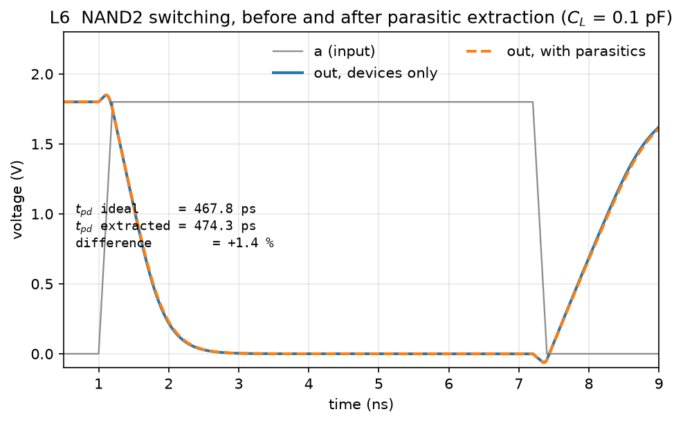 With a 0.1 pF load the two traces almost coincide: 467.8 ps against 474.3 ps,
a 1.4 % difference.
With a 0.1 pF load the two traces almost coincide: 467.8 ps against 474.3 ps,
a 1.4 % difference.
That looks like a disappointing result. It is the correct one, and the reason is the point of the exercise. Sweep the load and measure again:
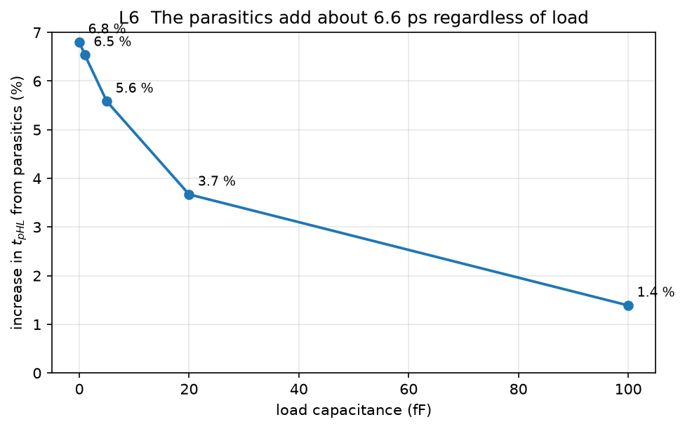 The parasitics add a roughly fixed 6.6 ps. Their share of the total delay is
6.8 % with no load and 1.4 % at 0.1 pF.
The parasitics add a roughly fixed 6.6 ps. Their share of the total delay is
6.8 % with no load and 1.4 % at 0.1 pF.
| \(C_L\) | ideal | extracted | change |
|---|---|---|---|
| 0 | 100.0 ps | 106.8 ps | +6.8 % |
| 1 fF | 104.0 ps | 110.8 ps | +6.5 % |
| 5 fF | 120.0 ps | 126.7 ps | +5.6 % |
| 20 fF | 177.1 ps | 183.6 ps | +3.7 % |
| 100 fF | 467.8 ps | 474.3 ps | +1.4 % |
Layout parasitics are an approximately fixed additive load. They dominate when a gate drives a short local wire and vanish into the noise when it drives a long one. Compare this against your P3 prediction.
Expected results
Submit the executed lab2.ipynb, with the layout plot attached.
- [ ] L2 — layout plot of your NAND2
- [ ] L3 —
drc count= 0 - [ ] L4 — extracted netlist showing four devices with the right W and L
- [ ] L5 — Netgen output reading Circuits match uniquely
- [ ] L6 — pre- and post-PEX waveforms, \(t_{pHL}\), \(t_{pLH}\), \(t_r\), \(t_f\) for both, and the delay-versus-load comparison with a written explanation
Extra notes
- The middle NMOS diffusion carries no contact. Series devices share diffusion directly; adding a contact there wastes area and adds capacitance to an internal node.
- Ignore the legacy handout's "L = 2 squares wide" annotation. Set the channel length from the poly stripe width, 0.5 µm.
- You do not have to match the reference layout's contact count. Dimensions matter; contact arrays do not.
- Magic reads commands on stdin even with the GUI open, which is the reliable way to script it:
FAQ
Failed to load technology.
No .magicrc in the directory you started Magic from. Create it as in L1.
The layout is one empty rectangle with a name in it.
An unexpanded subcell. Press x.
Every contact reports li.5.
The contacts have no local interconnect overhanging them. Paint li over a
rectangle 0.1 µm larger than each contact.
Netgen says Cannot find cell nand2 in file ….
The schematic netlist has no .subckt. Netlist a wrapper that instantiates
nand2.sym rather than nand2.sch itself.
LVS reports a pin mismatch but says the netlists match. The inputs are swapped. Rename the two poly labels in the layout.
The pre- and post-PEX waveforms look identical. They nearly are, at a 0.1 pF load — see L6. Reduce the load to make the difference visible, and report both.