Lab 1 — Basic SPICE simulations
ECE334 — Digital Electronics — SKY130 open-source flow
Objective
Use XSchem and ngspice to simulate four circuits, and analyse each result in Python. You start with an RC network, extract the device parameters \(K_P\) and \(V_t\) from a diode-connected transistor, characterise a CMOS inverter, and finish by building a pulse generator and sizing it for a specified pulse width.
Every section has two halves. Preparation is hand analysis, done before the lab session. Lab Work is the simulation that checks it. Bring the preparation with you; the lab is short if you have done it and long if you have not.
Course conventions
| Setting | Value |
|---|---|
| Process (PDK) | sky130A |
| Supply voltage | 1.8 V |
| Teaching channel length | L = 0.5 µm |
| NMOS / PMOS devices | sky130_fd_pr__nfet_01v8 / sky130_fd_pr__pfet_01v8 |
| Unit inverter | Wn = 1, Wp = 3 |
| NAND2 | Wn = 2 (series pair), Wp = 3 (parallel pair) |
| Extraction device (Lab 1 P2) | W = 10, L = 2 |
Widths and lengths are entered as unitless microns: W=1, L=0.5. A u
suffix means metres, lands outside every model bin, and makes ngspice report
"could not find a valid modelname".
The tools
| File | Purpose |
|---|---|
xschem/*_tb.sch |
Testbenches: stimulus, load, supply, and launcher buttons. You build your circuit inside the DUT. |
lab1.ipynb |
Your report. Loads each result, measures it, and holds your answers. |
spice/*.spice |
The same circuits as plain decks, if you prefer the command line. |
Start the environment, then:
Running a simulation
Use the Netlist and Simulate buttons at the right-hand end of the
menubar, in that order. Netlist writes <name>.spice; Simulate runs ngspice on
it and writes the .raw file the schematic's .control block names.
The green arrows inside each testbench do the same thing in one step, but they are launchers, and firing one takes two steps:
- click the arrow once — a box appears around its label, meaning it is selected;
- press
Ctrl-H.
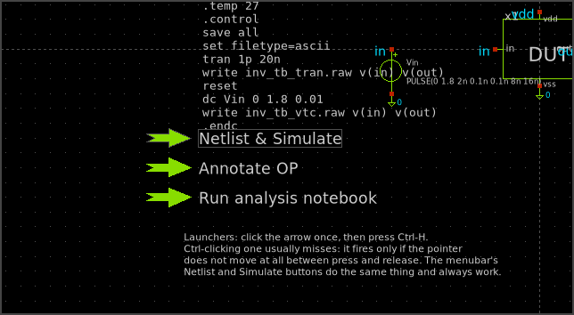
Netlist & Simulate has been clicked and is selected — note the box around
the label, which the other two do not have. Ctrl-H now fires it.
Ctrl-clicking a launcher usually does nothing
XSchem does have a Ctrl-click shortcut for this, and it only fires if the
pointer does not move at all between pressing and releasing the button.
Measured on this build, a 3-pixel drift is enough to lose it, which is more
than a hand on a mouse can avoid. It fails silently — no message, no
highlight. Use click-then-Ctrl-H, or the menubar.
A launcher also does nothing while anything else is selected, because it
acts only when the selection is exactly one object. Press Escape first if
you are not sure.
| Launcher | Equivalent |
|---|---|
| Netlist & Simulate | menubar Netlist, then Simulate |
| Annotate OP | Simulation → Annotate OP |
| Run analysis notebook | run lab1.ipynb in JupyterLab |
The notebook finds results by filename through sim.raw("rc_tb.raw"), so it
does not matter which directory you started XSchem from.
Net names
The testbench and the notebook agree through net names. Use these and the analysis works unchanged:
| Net | Meaning |
|---|---|
in |
stimulus input |
out |
the output you measure |
n3 |
chain output, P4 only |
vdd / vss |
1.8 V supply / ground |
A DUT is an empty box symbol carrying exactly these pins. Open it, build your circuit inside, and leave the pin names alone.
Preparation
P1 — RC divider
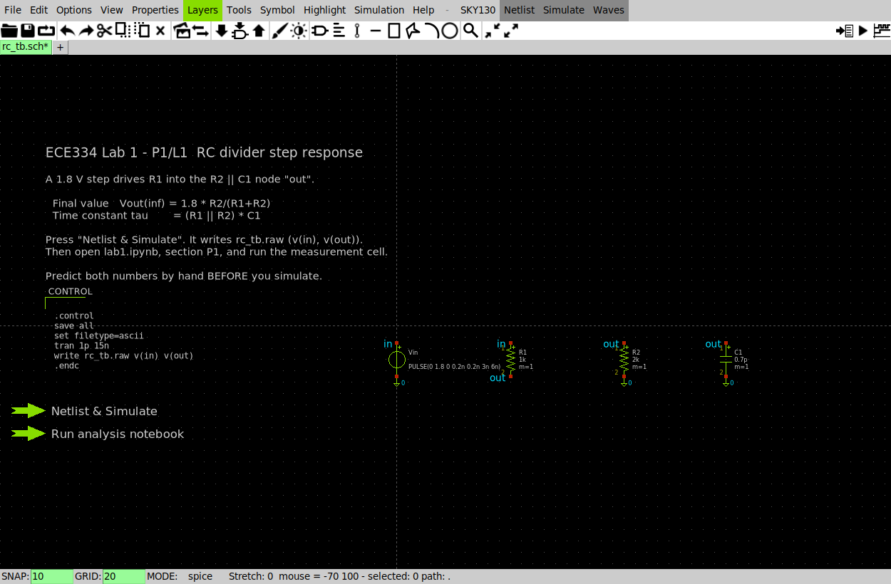
rc_tb.sch. The source, R1, R2 and C1 are wired by net name; the launcher
buttons are on the left.
A 1.8 V step drives \(R_1 = 1\ \mathrm{k}\Omega\) into the node out, which is
loaded by \(R_2 = 2\ \mathrm{k}\Omega\) in parallel with \(C_1 = 0.7\ \mathrm{pF}\).
The input pulse has \(t_r = t_f = 0.2\) ns, a width of 3 ns, and a period of 6 ns.
Derive, by hand:
Sketch \(V_{in}\) and \(V_{out}\) over the first 15 ns.
P2 — Device parameters
A diode-connected transistor has its gate tied to its drain, so \(V_{GS} = V_{DS}\) and the device is saturated whenever it conducts:
\(\sqrt{I_D}\) is therefore linear in \(V_{GS}\). Fitting a line to it over the strong-inversion region gives both parameters:
where \(m\) is the fitted slope. Write down how you will obtain \(K_P\) and \(V_t\) from a fitted slope and intercept before you run anything.
P3 — Inverter timing
Model a conducting transistor as a resistor:
The inverter's output then charges and discharges \(C_L\) exactly as the RC network in P1 did, so:
With \(W_n = 1\), \(W_p = 3\), \(L = 0.5\) and \(C_L = 0.2\) pF, compute \(R_{eq,n}\), \(R_{eq,p}\), \(t_r\) and \(t_f\). Leave \(K_P\) and \(V_t\) symbolic — you measure them in L2 and substitute afterwards.
P4 — Pulse generator
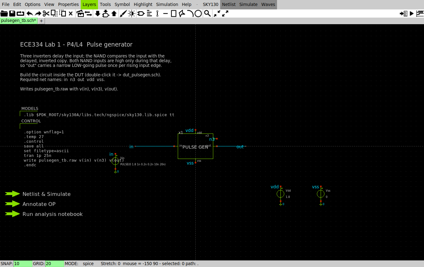
pulsegen_tb.sch. The DUT exposes n3, the chain output, so the testbench can
plot it beside in and out.
Three inverters in series feed one input of a NAND; the undelayed signal feeds
the other. Write the NAND truth table, then state what out does when in
rises, and explain why the resulting pulse width equals the delay of the
inverter chain.
Using your P3 expression for a single inverter's delay, write the pulse width in terms of \(R_{eq}\) and the capacitance at each chain node.
Lab Work
L1 — RC step response
Open xschem/rc_tb.sch, then click Netlist and Simulate in the
menubar. It writes rc_tb.raw.
Run section P1 of lab1.ipynb:
rc = sim.raw("rc_tb.raw")
t_rise, _ = measure.edges_10_90(rc, "out", vdd=1.2)
print(f"t_rise = {t_rise*1e12:.1f} ps,  tau = {t_rise/np.log(9)*1e12:.1f} ps")
plot.transient(rc, ["in", "out"])
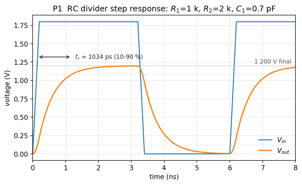 Measured 10–90 % rise time, 1034 ps. The output settles at 1.198 V, not the
1.8 V rail, because \(R_1\) and \(R_2\) divide it.
Measured 10–90 % rise time, 1034 ps. The output settles at 1.198 V, not the
1.8 V rail, because \(R_1\) and \(R_2\) divide it.
Compare against P1. The reference build measures:
| Quantity | Hand | Simulated |
|---|---|---|
| \(V_{out}(\infty)\) | 1.200 V | 1.198 V |
| \(t_r\) (10–90 %) | 1025 ps | 1034 ps |
| \(\tau\) | 466.7 ps | 470.8 ps |
Read \(\tau\) from \(t_r/\ln 9\) rather than from the 63.2 % point. The input takes 0.2 ns to rise, so there is no single instant the step "starts", and a 63.2 % reading taken from \(t = 0\) is about 16 % high.
Change \(R_1\) or \(C_1\), re-simulate, and confirm \(\tau\) tracks \((R_1\parallel R_2)C_1\).
L2 — Extract \(K_P\) and \(V_t\)
Open xschem/diode_tb.sch and build a diode-connected NMOS in the DUT: gate and
drain to g, source and body to s, W = 10, L = 2.
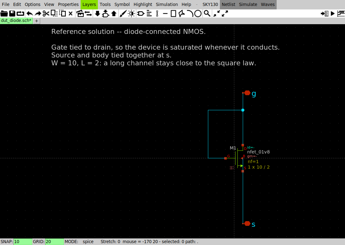
dut_diode.sch completed. The gate connects back to the drain; source and body
are tied at s.
Enter W and L without a u
Type W=10 and L=2, not W=10u/L=2u. The SKY130 models are binned on
plain micron numbers; a value in metres falls outside every bin and ngspice
stops with "could not find a valid modelname". This is the most common
first-simulation failure in this course.
Click Netlist then Simulate, and run section P2 of the notebook:
d = sim.raw("diode_nmos.raw")
res = measure.extract_square_law(d["g"], d["id"], wl=10/2, vmin=1.0, vmax=1.7)
print(res["Vt"], res["KP"])
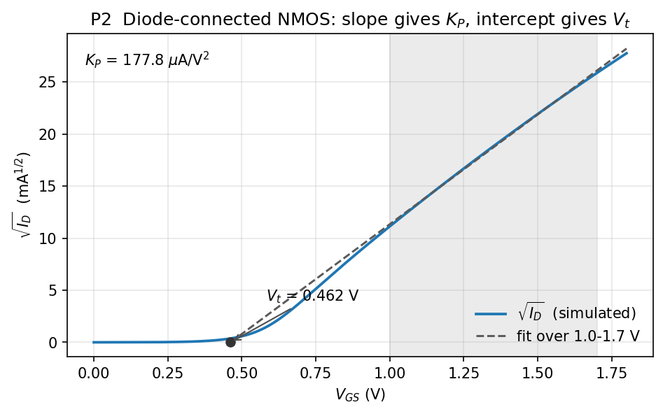 The fit is taken over 1.0–1.7 V (shaded), where the device is strongly
inverted. Extending it below about 0.8 V bends the curve and biases both
parameters.
The fit is taken over 1.0–1.7 V (shaded), where the device is strongly
inverted. Extending it below about 0.8 V bends the curve and biases both
parameters.
The reference build gives \(V_{tn} = 0.462\) V and \(K_{Pn} = 177.8\ \mu\)A/V². Repeat with a PMOS to obtain \(|V_{tp}|\) and \(K_{Pp}\). Record all four numbers — L3 and L4 need them.
Your values will differ slightly with the fit window. That is the point: the square law is an approximation to a short-channel device, and the parameters you get depend on where you fit it.
L3 — Inverter
Build the inverter in the DUT of xschem/inv_tb.sch: \(W_n = 1\), \(W_p = 3\),
\(L = 0.5\).
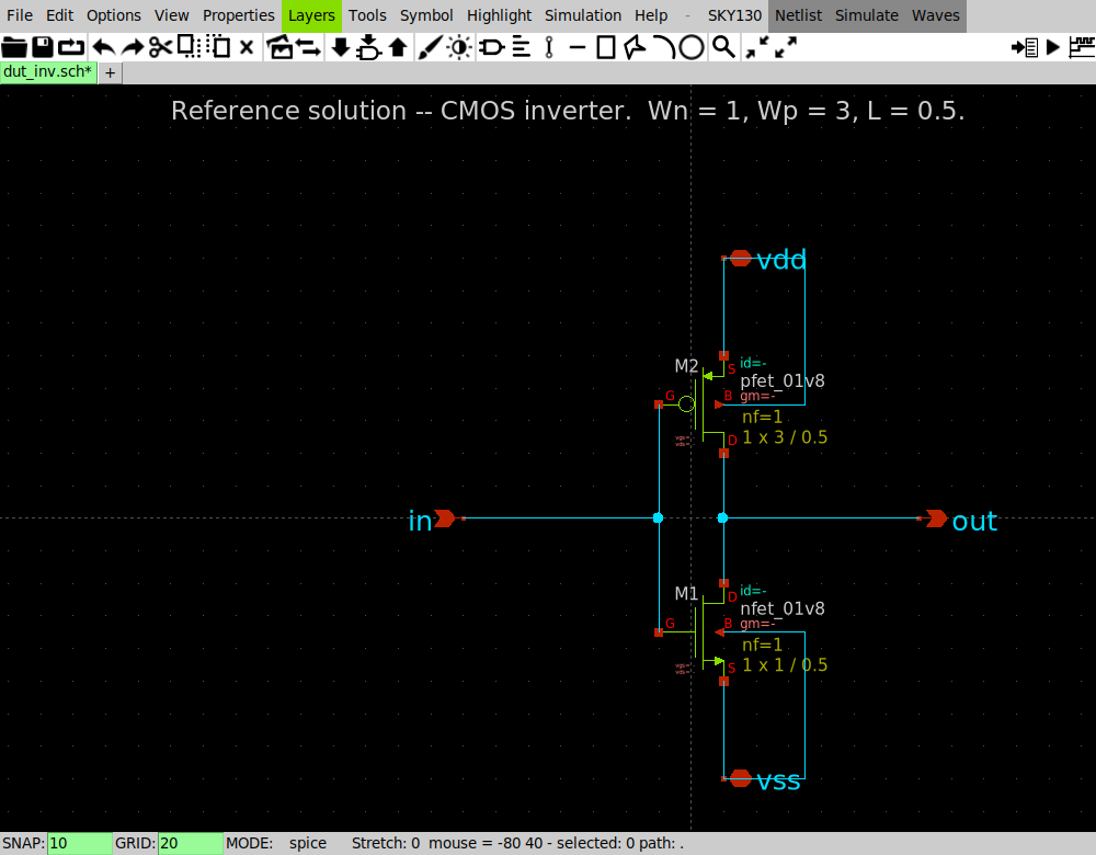
dut_inv.sch completed. PMOS source to vdd, NMOS source to vss, both
bodies tied to their own source, drains joined at out.
Selecting a device and pressing q opens its properties:
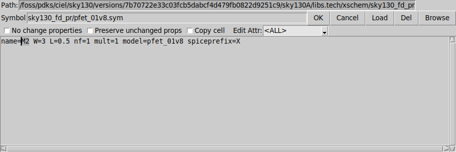
W=3 L=0.5 on the PMOS. spiceprefix=X and the diffusion geometry are filled
in by the symbol — you only set W and L.
Click Netlist then Simulate. It writes inv_tb_vtc.raw (DC sweep) and
inv_tb_tran.raw (transient).
Transfer characteristic. Run notebook section P3a:
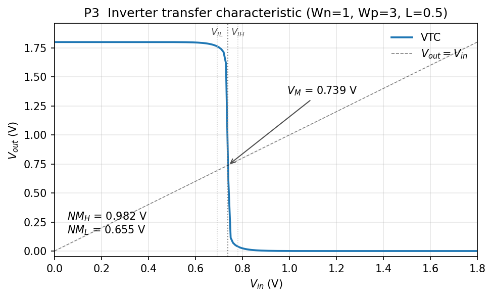 \(V_M = 0.739\) V, below mid-rail. \(NM_H = 0.982\) V and \(NM_L = 0.655\) V.
Report \(V_M\), \(NM_H\) and \(NM_L\). \(V_M\) sits below \(V_{DD}/2\): \(W_p/W_n = 3\) does not fully compensate the mobility ratio in this process. Say what you would change to move \(V_M\) to mid-rail, and what that costs.
Transient. Run section P3b:
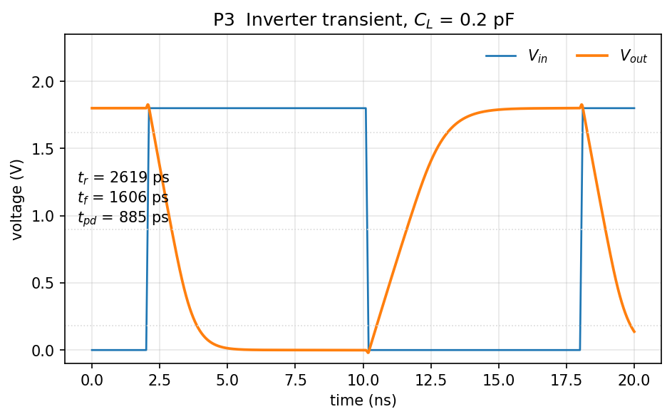 \(t_r = 2619\) ps, \(t_f = 1606\) ps, \(t_{pd} = 885\) ps with \(C_L = 0.2\) pF.
Substitute your extracted \(K_P\) and \(V_t\) into the P3 expressions and compare. The reference build gets \(t_r = 2801\) ps and \(t_f = 1665\) ps by hand against 2619 ps and 1606 ps simulated — within 7 %, and slightly conservative.
The agreement is that good because \(K_P\) came from a real device rather than from a datasheet, so the extraction already absorbed most of the short-channel behaviour. Say what would happen to the agreement if you fitted \(K_P\) over 0.5–1.0 V instead, and why.
L4 — Pulse generator
Build the circuit in the DUT of xschem/pulsegen_tb.sch from the inv and
nand2 cells in common/xschem. Press Shift-I to open the symbol browser.
Wire the last chain node to the n3 port.
Click Netlist then Simulate, and run notebook section P4:
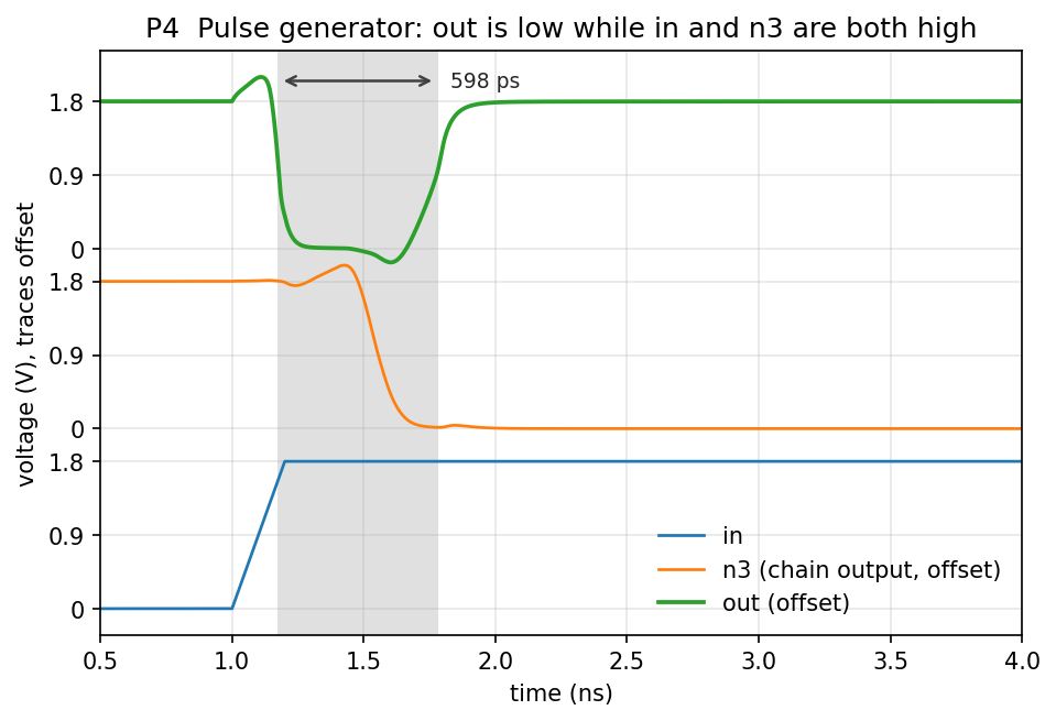
in rises; n3 is still high for the length of the chain delay; both NAND
inputs are high over that window, so out is low for 598 ps.
Measure the pulse width between the 50 % points. The reference build gives 598.4 ps. Compare with your P4 prediction.
Design task. Add a capacitor at n3 and size it so the pulse width is
1.5 ns. Work in three steps:
- Estimate. Only the falling edge of
n3closes the pulse, and the third inverter's NMOS drives that edge, so the extra delay is \(\approx 0.69\,R_{eq,n}C\). Compute the capacitance this predicts. - Calibrate. That estimate comes out about three times too large. It predicts roughly 2.6 ps of extra width per fF, while the circuit delivers about 7.1 ps/fF, so far less capacitance is needed than the model claims. \(R_{eq}\) is the resistance at full gate overdrive; the real device spends much of the transition with less drive and out of saturation. Simulate at two capacitances, measure both widths, and interpolate for 1.5 ns.
- Confirm. Use the interpolated value and check the width.
The reference build needs ≈ 128 fF and measures a sensitivity of about 7.1 ps/fF: 0 fF → 598 ps, 40 fF → 905 ps, 80 fF → 1184 ps, 120 fF → 1450 ps.
Report all three numbers — the estimate, the interpolated value, and the measured width — and say why step 1 was off. Trial and error with only a final number is not sufficient; explaining the gap is the exercise.
Expected results
Submit the executed lab1.ipynb. It must contain, for each section, your hand
analysis, the measured value, and a written comparison.
- [ ] L1 — \(V_{in}\) and \(V_{out}\) plot; measured \(\tau\) and \(t_r\) against P1.
- [ ] L2 — NMOS and PMOS fits; \(V_{tn}\), \(K_{Pn}\), \(|V_{tp}|\), \(K_{Pp}\).
- [ ] L3 — VTC with \(V_M\), \(NM_H\), \(NM_L\); transient \(t_r\), \(t_f\), \(t_{pd}\) against the P3 estimate built from your own parameters.
- [ ] L4 — pulse-generator waveforms and measured width; the capacitor you predicted for 1.5 ns and the width you achieved.
Extra notes
- Rise and fall times are 10–90 % unless stated otherwise. Propagation delay is 50 % input to 50 % output. Pulse width is 50 % to 50 %.
- The pulse from this circuit is low-going: measure from the falling edge to the following rising edge.
- Both routes run the same circuit.
spice/pulsegen.spicereproducespulsegen_tb.schincluding the diffusion geometry the XSchem symbols generate for you; both give 598.4 ps. A hand-written deck that omitsad/as/pd/psruns about 25 % fast. - To check your files before a demo: It netlists and simulates every testbench and fails loudly on an empty DUT.
FAQ
ngspice says "could not find a valid modelname".
A width or length has a u suffix. Use W=1, L=0.5.
The netlist contains IS MISSING !!!! and no transistors.
XSchem cannot find a symbol. Re-run . /foss/designs/common/.designinit, which
reinstalls the course configuration at ~/.xschem/xschemrc, then reopen the
schematic.
verify_lab.sh says "empty subcircuit(s) … the DUT has not been built yet".
The testbench is fine; the DUT behind it is still the empty stub. Click the DUT
once to select it, then press e to descend into it, and build the circuit
there. (Double-clicking opens the Edit Properties dialog instead.)
write fails with "no writable vector found".
Same cause seen from ngspice's side: the nets named in the .control block do
not exist because the DUT is empty.
The notebook cannot find a .raw file.
Netlist and simulate the testbench before running the cell. Results go to
/foss/designs/.xschem/simulations, and sim.raw() looks there and in the
current directory.
My extracted \(K_P\) and \(V_t\) differ from the numbers above. Expected. They depend on the fit window and on which device you swept. Use your own values throughout, and say which window you used.