Inductors on a chip
Resistors and capacitors on a chip both turned out to be shapes you draw, so you might expect an inductor to be a spiral you draw too. It is, but that spiral is both a poor inductor and an enormous one, and both problems have the same underlying cause, which the end of this page explains.
So far every passive on a chip has been “a shape, and the shape costs area”. Inductors don’t fit that pattern, because although you can draw one and the foundry will make it, at most frequencies what you get back behaves like a resistor.
The three SKY130 inductor models
SKY130 models exactly three spiral inductors. They live in libs.ref/sky130_fd_pr/spice/, and unlike everything else in this course they aren’t loaded by sky130.lib.spice, so you have to .include them yourself:
sky130_fd_pr__ind_03_90.model.spice
sky130_fd_pr__ind_05_125.model.spice
sky130_fd_pr__ind_05_220.model.spice
Warning: if you forget the
.include, ngspice saysError: unknown subckt: x1 a 0 ct 0 sky130_fd_pr__ind_05_220 Simulation interrupted due to error! Error: incomplete or empty netlistThat error means the netlist is missing the inductor’s model file, and the PDK itself is fine.
The subcircuit in sky130_fd_pr__ind_05_220.model.spice is fourteen lines long:
.subckt  sky130_fd_pr__ind_05_220 a b ct sub
R31 net27 b r='1e-2'
R26 a net23 r='1e-2'
C2 net27 net31 c='223.7e-15'
C24 net35 net27 c='205e-15'
C25 net23 net37 c='223.7e-15'
R5 sub net31 r='5.358e3'
R4 net41 net27 r='2.059'
R13 net23 net35 r='9.064'
R10 sub net37 r='5.358e3'
R9 net23 net39 r='2.059'
    L1 net39 ct l=4.96e-9
    L3 ct net41 l=4.96e-9
.ends
There are two inductors of 4.96 nH, one on either side of the centre tap ct, so the total is 9.92 nH. Around them are 4.138 Ω of series resistance (2.059 + 2.059 + 0.01 + 0.01); 447.4 fF of coupling into the substrate, as two 223.7 fF capacitors each draining through 5.358 kΩ into the sub terminal; and 205 fF directly across the winding, in series with a 9.064 Ω resistor (R13).
Only two of its twelve elements are inductors. The other ten describe the losses and parasitics, and the rest of this page is about what they do to the device.
Q
The figure of merit for an inductor is its quality factor:
\[Q = \frac{\operatorname{Im}(Z)}{\operatorname{Re}(Z)} \approx \frac{\omega L}{R_{s}}\]
An ideal inductor has \(Q = \infty\) and a resistor has \(Q = 0\), so Q tells you how much of the component is actually behaving as an inductor.
labs/passives-decks/spice/l_spiral.spice measures ind_05_220 at four frequencies:
--- ind_05_220: L (H), Q, series R (ohm) at four frequencies ---
l_1khz              =  9.91271e-09
q_1khz              =  1.50516e-05
r_1khz              =  4.13800e+00
l_1mhz              =  9.91271e-09
q_1mhz              =  1.50516e-02
l_100mhz            =  9.92203e-09
q_100mhz            =  1.50196e+00
l_1ghz              =  1.07762e-08
q_1ghz              =  1.16534e+01
At 1 kHz, Q is 0.0000150516, which means that at audio frequencies the largest inductor SKY130 offers is 99.9985 % resistor: a 4.138 Ω resistor with a trace of inductance attached. Nothing in the circuit can change that, because \(Q = \omega L/R\) and you don’t get to choose \(\omega\).
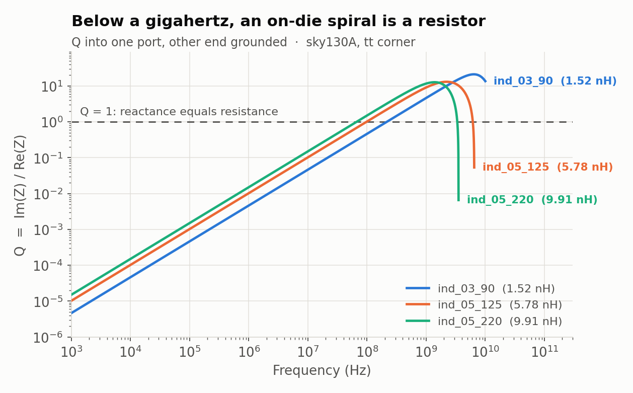
Each line is straight on these log–log axes because Q is proportional to frequency, so every decade up multiplies Q by ten. That rise is the reason on-die inductors exist at all: at 2.4 GHz they are useful, and every Wi-Fi and Bluetooth radio ever made has spirals in its LC oscillator. Below about 100 MHz they take up space and do nothing useful.
--- best Q each spiral ever reaches, and where ---
qpeak_03_90         =  2.11268e+01 at=  6.38263e+09
qpeak_05_125        =  1.30871e+01 at=  2.21309e+09
qpeak_05_220        =  1.27198e+01 at=  1.38835e+09
The best any of them manages is Q = 21.1, from ind_03_90, and it gets there only at 6.38 GHz. Compare that with the resistor you have been simulating all course, whose value you can hit to five digits.
You’ll run this deck, and the Lab 02 inductor sweep, in Lab 02, Part 7.
Self-resonance
The 223.7 fF capacitors in the model resonate with the inductance, and above the resonant frequency the whole structure behaves like a capacitor. Here is that frequency for two of the spirals:
--- self-resonance: the frequency where it stops being an inductor ---
srf_05_125          =  6.49382e+09 with=  1.99663e+03
srf_05_220 = 3.52777e+09 with= 2.18171e+03(meas ac also prints the value it was searching on; the frequency is the first number.)
Above 3.52777 GHz the reactance of ind_05_220 changes sign, and on the Q plot all three curves drop off sharply at the high-frequency end. That leaves ind_05_220 barely a decade and a half of usable band, from 100 MHz, where Q is still only 1.50, up to 3.53 GHz, where it stops being an inductor at all. Its peak Q in that band is 12.7.
Area
The ind_* files are electrical models with no layout attached, but SKY130 does ship drawn spirals: three RF test coils inside libs.ref/sky130_fd_pr/gds/sky130_fd_pr.gds. They are separate PDK objects from the three models, with different names and characterisation, but they are the same kind of structure, and they are the only on-die inductors this process has drawn. These are their bounding boxes, measured with KLayout:
| cell | footprint | area |
|---|---|---|
sky130_fd_pr__rf_test_coil1 |
150.020 × 145.040 µm | 21 758.9 µm² |
sky130_fd_pr__rf_test_coil2 |
270.000 × 265.000 µm | 71 550.0 µm² |
sky130_fd_pr__rf_test_coil3 |
370.080 × 365.080 µm | 135 108.8 µm² |
Here is the middle one, rendered from that GDS with the SKY130 KLayout layer properties:
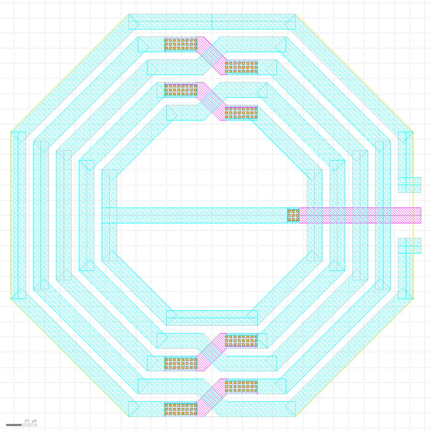
It is made of concentric octagonal turns of met3 (cyan, 32 806.81 µm² of it), with met2 crossunders (magenta) where the winding has to cross itself, and 201 arrays of via2 joining the two layers so both metals carry the current in parallel. The bar running out through the middle is the third terminal, the same centre tap the netlist calls ct. The whole thing sits inside a marker on a layer named inductor.drawing (GDS 82/24), which tells the foundry’s tools not to put anything underneath it.
Here is the same picture with forty-nine sky130_fd_sc_hd__inv_1 standard cells placed in the middle, at the same scale:
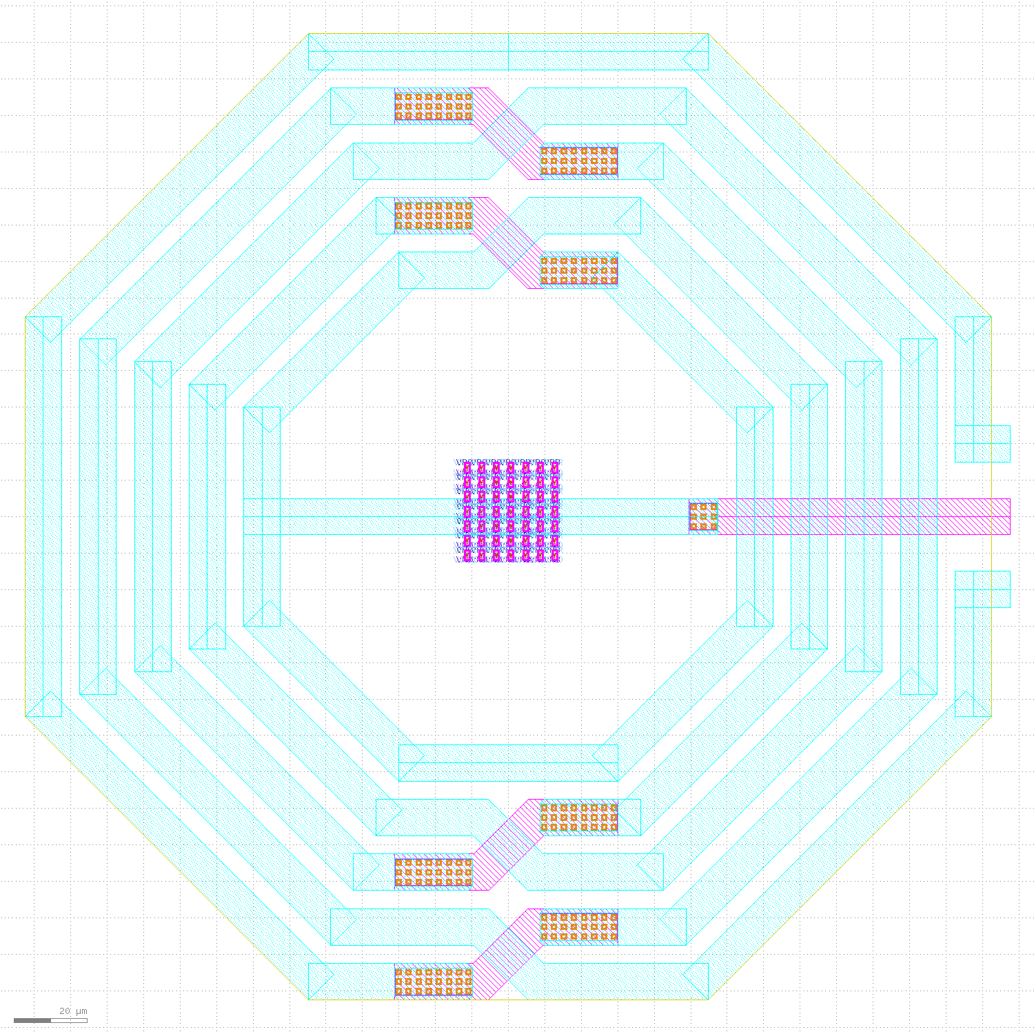
You can barely see the inverters, because inv_1 is 3.7536 µm² and the coil is 71 550 µm². One inductor takes the area of 19 062 inverters, a small CPU’s worth of silicon, for single-digit nanohenries and a Q in the low teens, in a frequency band you probably weren’t using.
Why spirals are large and lossy
An inductor stores energy in a magnetic field in the space around the wire. A capacitor stores energy in an electric field across a gap you can make 4 nanometres thick, and a resistor is a strip whose length you control. A magnetic field has no thin-film equivalent: to get inductance you need area enclosed by current, and the only way to get that is to spend square micrometres. The field also goes straight down into the silicon substrate, which conducts, so it induces eddy currents. In the model the substrate is the sub terminal, and the only elements connected to it are the two 5.358 kΩ resistors, each behind a 223.7 fF capacitor. Both problems come from the same field, so you can neither make an inductor small nor stop it coupling to the wafer it is printed on.
That’s why bond wires and package traces are sometimes used as the inductor instead. A 1 mm bond wire is roughly a nanohenry, and because it sits in the package rather than on the die, it costs no silicon.
Inductors below a gigahertz
If your circuit needs an inductor below a gigahertz, the circuit is wrong for a chip. The fix has to go in the circuit rather than the layout.
No layout trick, fold or metal stack fixes \(Q = 1.5\times10^{-5}\) at 1 kHz, so you change the topology instead. Analog designers have been working around this since the 1960s, and there is a mature set of replacements.
Next on the Course path: Lab 02: How big is a picofarad?. After that, What to build instead of an inductor covers the replacements.