What a resistor costs in area
If a resistance on a chip is just a length of material, it’s fair to ask how long a real one has to be, and whether that length is a problem. This page works out the numbers.
Ohms per square gives the resistance of sky130_fd_pr__res_high_po, drawn 1 µm wide, as a function of its length:
\[R(L) = 378.2448 + 317.2198\,L \qquad (L \text{ in µm})\]
If you solve that for \(L\), it becomes a design procedure: to get a resistance \(R\), you draw a length
\[L = \frac{R - 378.2448}{317.2198}\]
Three values, sized and simulated
Section B of labs/passives-decks/spice/r_head_and_body.spice, the same deck Ohms per square uses, sizes three resistors this way and simulates them:
| you want | \(L\) from the formula | ngspice says |
|---|---|---|
| 1 kΩ | 1.960014 µm | 1000.000 Ω |
| 10 kΩ | 30.331509 µm | 10 000.00 Ω |
| 100 kΩ | 314.046460 µm | 100 000.0 Ω |
--- B. sized to 1 k, 10 k, 100 k (ohms) ---
r_1k = 1.000000e+03
r_10k = 1.000000e+04
r_100k = 1.000000e+05
The formula and the simulator agree, and the last row says that a 100 kΩ resistor is a strip of polysilicon 314 micrometres long.
To get a sense of scale, compare it with the smallest inverter in the SKY130 standard-cell library, sky130_fd_sc_hd__inv_1, which has area : 3.7536 µm² in libs.ref/sky130_fd_sc_hd/lib/sky130_fd_sc_hd__tt_025C_1v80.lib. Your 100 kΩ resistor is 314.046460 × 1 µm = 314.05 µm² of drawn poly, which is the silicon of 84 inverters. So a passive component you wouldn’t think twice about on a breadboard costs as much floor space as a small logic block.
Larger values get expensive quickly, because the length grows in proportion to the resistance. A 1 MΩ resistor in the same material at the same width needs
\[L = \frac{10^6 - 378.2448}{317.2198} = 3151.2\ \text{µm} = 3.15\ \text{mm}\]
which is longer than many whole dies. Folding (later on this page) won’t rescue a resistor that size, so instead you redesign the circuit so that it doesn’t need one.
Width and area
How every on-chip resistor gets drawn follows from rearranging the resistance formula. For a fixed resistance, the length you need is proportional to the width, so
\[L \propto R\,W \quad\Longrightarrow\quad \text{area} = W L \propto R\,W^2\]
and the area goes as the square of the width. If you draw a resistor twice as wide, it has to be twice as long to keep the same resistance, so you pay for four times the silicon. Section D of the deck builds the same 100 kΩ at four more widths to check this:
--- D. 100 k at four widths (ohms), and the area each one costs ---
r_w0p35 = 9.999975e+04
r_w0p69 = 1.000002e+05
r_w2 = 9.999982e+04
r_w5 = 1.000004e+05| \(W\) (µm) | \(L\) (µm) | ngspice (Ω) | area \(WL\) (µm²) | in inv_1s |
|---|---|---|---|---|
| 0.35 | 101.9319 | 99 999.75 | 35.68 | 9.5 |
| 0.69 | 216.2792 | 100 000.2 | 149.23 | 39.8 |
| 1 | 314.046460 | 100 000.0 | 314.05 | 83.7 |
| 2 | 629.5313 | 99 999.82 | 1 259.06 | 335.4 |
| 5 | 1576.1560 | 100 000.4 | 7 880.78 | 2 099.5 |
Every row gives the same value to five digits, yet the bottom row takes 221 times the area of the top row. The square law on its own predicts \((5/0.35)^2 = 204\). Most of the rest comes from the 0.35 µm strip, which the model treats as slightly narrower than drawn, so it has about 7 % more ohms per square than the wider ones and needs less length (Lab 01, Part 4 measures this). Its larger end resistance shortens it a little more.
So draw a resistor at the narrowest width that the design rules and your accuracy budget allow. For res_high_po, the narrowest width SKY130 permits is 0.35 µm. Make it wider only when you have a reason to, such as better matching (Matching and Pelgrom’s law) or carrying more current.
Changing the material
You choose the width and length freely, but the material has to come from the short list the process offers. Section C of the deck draws the same 314.046460 × 1 µm strip with four different implants:
| model | value | Ω/□ (measured) |
|---|---|---|
res_generic_nd (n+ diffusion) |
36.89775 kΩ | 117.5 |
res_generic_pd (p+ diffusion) |
61.38915 kΩ | 195.5 |
res_high_po |
100.0000 kΩ | 317.2198 |
res_xhigh_po |
665.3872 kΩ | 2118.7619 |
res_xhigh_po gives 6.7 times as many ohms per micron of length, so the 1 MΩ resistor shrinks from 3.15 mm to
\[L = \frac{10^6 - 34.2111}{2118.7619} = 472.0\ \text{µm}\]
That’s still big (472 µm² of poly at 1 µm wide, or 126 inverters), but it fits on a die.
Why 2118.7619 and not 2000. The
res_xhigh_pomodel card saysrsheet = 2000.0, but it also saysweff = {w-0.056}, which means the strip comes out of the fab 56 nm narrower than you drew it, because the etch undercuts the edge. At a drawn W = 1 µm the material is really 0.944 µm wide, so the resistance per micron of length is \(2000 / 0.944 = 2118.6441\ \Omega\). Lab 01 measures 2118.7619, which agrees to four digits; the small remainder is the model’s nonlinear body term. Afterleffon Ohms per square, this is the second place in the course where what you drew and what you got differ by an amount you can calculate, and Process corners is about that gap.
Folding a long resistor
A strip 314 µm long and 1 µm wide doesn’t fit anywhere sensible on a die, so real layouts fold it. You might draw sixteen strips of 20 µm side by side, for example, and join them end to end with short turns of the same poly, so the current runs back and forth like a plough across a field. Folding shifts the value, though. The straight runs still count square for square, but the current cuts across the inside of each corner, so a corner square counts as only roughly half a square, and you have to re-tune the length to bring the folded strip back to the value you sized it for. Folding also makes you pay for:
- the required spacing between neighbouring poly strips;
- a guard ring, if the resistor needs isolating from its neighbours;
- dummy strips at each end, which are extra resistors connected to nothing. Etching behaves differently at the edge of a pattern than in the middle, so a dummy gives the outermost real strip the same surroundings as the inner ones, and the edge effect falls on a device nobody uses.
Drawn straight, a resistor is the rectangle the formula describes: a bar of poly with one contact at each end.

Folded, it’s the same bar laid back and forth. The poly itself turns each corner, and there are still only the two contacts, one at each end:
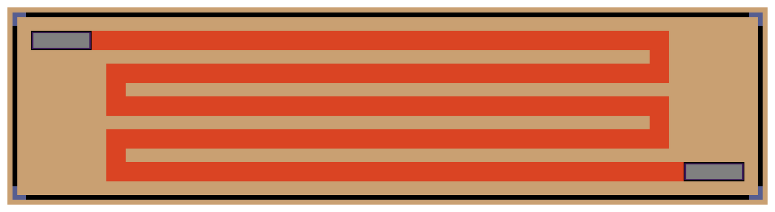
This one has five passes rather than the sixteen the 100 kΩ above would need, since the figure is there to show the shape, not the count. The red is the resistor body, and the grey blocks at the ends are its contacts. Each turn you add buys you height and costs you two corners.
A folded 100 kΩ resistor with its guard ring and dummies typically occupies two to three times its 314 µm² of drawn poly. Nobody publishes an exact multiplier, because it depends on the number of folds and on the spacing rules. The spacing alone goes a long way: the SKY130 device generator that Magic uses (/foss/pdks/sky130A/libs.tech/magic/sky130A.tcl) keeps 0.48 µm between neighbouring res_high_po strips and 0.48 µm between a strip and its guard ring, so in a fold of 1 µm strips every strip brings a gap half its own width.
If you’d like to see the layers in “a strip of poly with two contacts”, you can draw one in SiliWiz, a layout tool that runs in the browser and shows the cross-section as you draw. That’s the optional Lab 01, Part 9.
How this shapes analog circuits
These numbers shape every analog block you’ll read about. Bias networks use ratios of small resistors instead of one big one, and bandgap references use a handful of matched units rather than one exact value. Filters that would need a megohm on a breadboard are built from switched capacitors instead (What to build instead of an inductor). Designers work this way because a 100 kΩ resistor costs as much silicon as 84 inverters.
Next on the Course path: Lab 01: A resistor you designed. After that, Capacitors on a chip asks the same question about capacitors, and the area bill is much bigger.