Boards for chips: carriers, motherboards and characterization boards
This page answers: the Pmod you drew is one kind of board a chip needs. What are the others, and what does each ask of you that a Pmod didn’t?
The Pmod you drew in Labs 03 and 04 plugs into Tiny Tapeout’s demo board, and the demo board does a lot of the work for it. The demo board powers the chip, selects the project through the multiplexer on the chip, usually provides the clock, and reaches every project pin through its DIP switches, its 7-segment display, its Pmods and its RP2350. Your Pmod adds only the hardware that one project needs on top of all that, which is why it made a good first board. The other boards that a team ends up needing take over more of the demo board’s jobs, or carry a different chip altogether. This page goes through them in order, from the kind closest to what you’ve done to the kind furthest from it, so that when the team needs one you’ll know what it involves. The capstone’s two briefs are a Pmod and the first kind below, a board that drives one of the chip’s analog pins.
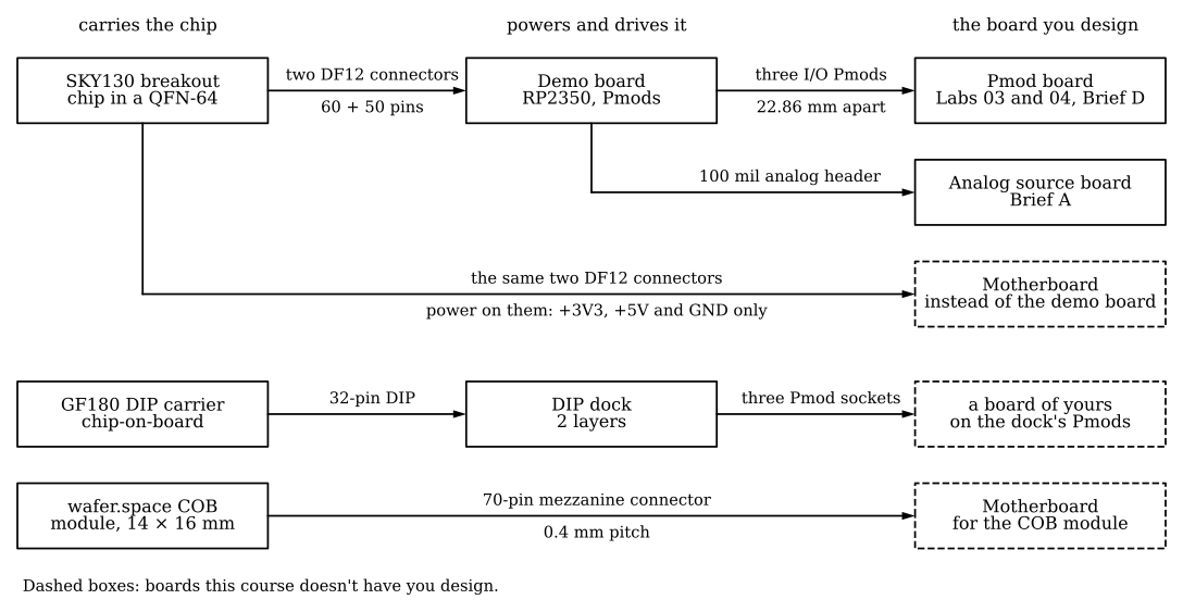
Where each kind of board attaches, from the chip outwards. The solid boxes are boards that exist, or that you design in this course; the dashed ones are boards a team could design next. Made by scripts/figures/board_kinds.py.
A board for an analog pin
CrossWalk, one of the team’s designs, is an 8-bit SAR ADC with two analog pins (its info.yaml says analog_pins: 2 and clock_hz: 4000000). Testing it means driving an analog pin with a voltage you know, cleanly enough that the converter’s errors aren’t hidden under the source’s.
On the demo board, each analog line comes out on a 100 mil header and is “pulled down with a large 10 MegaOhm resistance”. The SKY130 chips have 12 pins for analog, and a project may use up to 6 of them (demo board guide). Inside a SKY130 chip, each of a project’s analog pins is connected to its pad through an analog switch, tt_asw_3v3, and Tiny Tapeout’s analog spec gives the limits of that path as “Resistance: < 500 ohm”, “Capacitance: < 5 pf” and “Max current: 4 mA”.
A source board’s design note starts from those numbers. The two examples of the arithmetic below are ours rather than Tiny Tapeout’s.
- The 10 MΩ pull-down and your source’s output resistance form a voltage divider. A source with 10 kΩ of output resistance loses 10 kΩ / 10 MΩ = 0.1 % of its voltage, which is a quarter of one step of an 8-bit converter (1/256 is 0.39 %). A buffered source has an output resistance of a few ohms, so it loses a millionth of its voltage or less, far less than a step.
- The path’s resistance and capacitance set a time constant. With only the path’s own 500 Ω and 5 pF it’s 2.5 ns, but a 10 kΩ source charging the same 5 pF makes it 50 ns. Settling to within half a step of 8 bits (1/512) takes ln 512 ≈ 6.2 time constants, about 310 ns, which is longer than one 250 ns cycle of CrossWalk’s 4 MHz clock. So if CrossWalk samples its input for a single clock cycle, a 10 kΩ source won’t have settled by the end of it.
The capstone’s Brief A is the simplest form of this board. It drives one analog pin from a known, filtered source, has a test point on the source and one on the pin, and comes with a design note that does the arithmetic above for your own parts.
A full characterization board, which measures how good the converter is, is a bigger design, and we’ve left it for PCB201, a second course that would follow this one. Such a board needs a test signal that is more linear than the converter it tests. Steve Arar’s article on the sine-wave histogram method (All About Circuits, October 20, 2023) uses a sine for this and not a ramp, because “the linearity of the ramp signal produced by typical signal generators is limited to 8 to 10 bits”, which is not much better than an 8-bit converter itself, while “we can filter out the harmonics of a sinusoidal signal”. You drive the converter with a sine slightly larger than its full-scale range, so that “we can be sure that the input exercises all codes” (the article’s example puts 1.1 V on a 1 V converter). The sine’s frequency mustn’t be a subharmonic of the sampling rate, and the example uses 390.3 Hz against 40 kHz, with 80,000 samples. You then count how often each code appears and divide each count by the count an ideal converter would give, and “Subtracting one from the bin counts therefore produces the DNL information.”
The board also needs a voltage reference of its own. Horowitz and Hill describe a programmable laboratory source built around a DAC, and they write that in a circuit like that the voltage reference is usually the biggest source of noise. The ADR445 that they chose for it has about 2 µV peak-to-peak of noise from 0.1 to 10 Hz (The Art of Electronics, 3rd ed., chapter 13).
There’s no CrossWalk silicon to test yet. CrossWalk is tagged for Tiny Tapeout’s TTSKY26d shuttle, which closes on 2026-11-30. Its chips are expected on 2027-05-25, and the estimated shipping date is 2027-06-25 (chips page). Until then a board for CrossWalk is a design exercise, but if you design it now, while the chip is still being designed, the chip and the board can each still change to suit the other.
A motherboard for the breakout
For anyone making their own board, Tiny Tapeout’s FAQ says “we recommend that you design your PCB to interface with our breakout board”, and that the breakout “will provide you with 2 connectors where you get all of the signals of the chip.” A board that mates with the breakout’s two DF12 connectors takes the demo board’s place, so it has to do all of the demo board’s jobs: power the breakout, select the project through the chip’s multiplexer, provide the clock and reset, and drive and read the pins.
It can’t reach the chip’s own supplies, though. We followed every power net of the SKY130 breakout (rev 3.2, breakout-pcb at 91a2bf1), and the only supplies on its two connectors are +3V3, +5V and ground. The 60-pin connector J1 has one +3V3 pin and 24 ground pins, and the 50-pin J3 has two +5V, two +3V3 and 13 ground. The chip’s three rails stay on the breakout. VCCD (1.8 V) comes from the breakout’s one fitted regulator through a 0 Ω link, and VDD_IO and VDDA come from +3V3 through 0 Ω links. So a motherboard can measure the breakout’s total current on +3V3, and it can change VDD_IO and VDDA together by changing +3V3, but it can’t measure or change one rail on its own. For that you’d need the rework that the breakout’s silkscreen describes: taking off an 0805 link and fitting the header J2, which isn’t fitted on the boards Tiny Tapeout ships (Bringing up a chip shows its empty pads). That rework is on the board that carries the kit’s only chip, so if the team ever needs it, practise first on a breakout without a chip.
Drawing a motherboard is more work than drawing a Pmod, too. Tiny Tapeout’s breakouts and demo board all have 4 copper layers, and the DF12 connectors have a 0.5 mm pitch, both the breakout’s (their footprints are HRS_DF12NB-60DS-0.5V_51 and HRS_DF12NB-50DS-0.5V_51) and the mating halves that the demo board carries and a motherboard would need. That’s far finer than anything this course has you solder (Parts you can solder by hand). And because the motherboard now selects the project, the multiplexer’s control lines are yours to get right. Tiny Tapeout got two of them wrong on its own TT07 breakout, which, in the README’s words, “has the ASIC project MUX reset_n and increment wires crossed and is thus mislabelled”.
A motherboard also has to make the clock, which on the demo board is usually the microcontroller’s job. On the RP2040 version of the demo board, the microcontroller could “generate the clock signal for your design, up to 50 MHz” (PCB spec). Tiny Tapeout’s GPIO spec gives the official limits of the SKY130 pins as 33 MHz for an output and 66 MHz for an input, and it reports a worst-case round trip through the multiplexer of 20 ns, measured on TT3.5 silicon. A motherboard that clocks the chip itself, or reads back an output in the same clock cycle, has to stay inside those numbers.
Boards for chips from other shuttles
The team’s chip designs so far are all on Tiny Tapeout’s SKY130 and IHP shuttles, which deliver each chip in a QFN on a breakout. Other ways of getting a chip made deliver the die mounted on something else, or not mounted at all, and the board you’d design around it changes with that.
Tiny Tapeout’s GF180 shuttles
These shuttles don’t package the die. In the FAQ’s words, they “have the die bonded to a PCB directly (called chip-on-board, or COB)”. Tiny Tapeout’s “TT GF180 CoB DIP Breakout” carries the die on a board in the shape of a 32-pin DIP, and brings out “all the I/O (8 in, 8 out and 8 bidirectional)”, “the project clock and reset” and “the Tiny Tapeout project MUX, to select the design”. It also has a CH32X035 microcontroller that can select designs and clock projects, though you can leave both jobs to the board that the breakout plugs into instead. That board is the DIP dock, whose fabrication files you went through in Fabrication outputs. Its README says it “is very simple, and designed using only two layers”, and it has the same DIP switches, 7-segment display, Pmods, and manual clock and reset as the demo board. It’s a board you could have drawn after Lab 03.
wafer.space
wafer.space runs shuttles on GF180MCU, and each slot you buy on one gets you 1,000 dies. On November 16, 2026, its site listed Run 3 at $8,000 for a 3.93 × 5.12 mm slot, with a purchase deadline of 9 December 2026 and parts shipping in Q2 2027. Chip-on-board packaging was a $1,500 add-on ($1.50 per die) that “Requires the default pad ring for wire bonding”, and the site listed no QFN option.
wafer.space’s chip-on-board repository (Apache-2.0) shows what the board side of that looks like. For a full slot, the die is bonded to a 14 × 16 mm breakout with 74 pads, following “the Tiny Tapeout convention of 74 pads”, and the breakout plugs into a motherboard through a 70-pin mezzanine connector with a 0.4 mm pitch. The repository has example motherboards in KiCad.
The repository’s table for Run 1 maps each bond pad on the die to a pad on the breakout and to a Tiny Tapeout function. Bond pad 0 goes to breakout pad 1, ctrl_ena; bond pads 9 to 16 go to breakout pads 10 to 17, uo[0] to uo[7]; bond pads 19 to 24 carry analog[0] to analog[5]; and bond pads 17 and 73 are VDD IO. The wire-bonding rules for Run 1 say “No wires may cross”, “Wire angle must be not greater than 45°” and “Maximum wire length must be less than 3 mm”. A wire must also be at least 1 mm long or twice the die thickness, whichever is greater, and “No solder mask is allowed in the area to be bonded”. wafer.space calls wire bonding “a very manual process”, because “there are no real exchange formats yet that tie the die layout to the breakout PCB”. To help, it wrote a script that reads the die’s GDS file and the breakout’s KiCad file together and “walks pin-for-pin around the padframe” to match each pad on the die to its bond pad on the board.
ChipFoundry’s chipIgnite
ChipFoundry’s chipIgnite shuttles are on SkyWater 130. A tapeout costs “$14,950” for up to 15 mm² of die with “38 fully -configurable I/Os”, and it comes with an evaluation board and the “Option of 100 QFN-packaged parts or Bare Die”. The CI2612 shuttle tapes out on December 7, 2026, for delivery on May 25, 2027. A QFN from chipIgnite would need a board much like Tiny Tapeout’s breakout, decoupling and all, and that’s a board for PCB201 rather than this course.
A bare die of your own
Packaging a bare die locally is possible. The Toronto Nanofabrication Centre’s January 2026 price list has a TPT HB16 wire bonder at $49 an hour for UofT users, and staff service at $60 an hour from 9 am to 5 pm. CMC Microsystems packages dies in DIP 40, CFP 24, CQFP 44, 80 and 120, and CPGA from 69 to 209 pins. It also wire-bonds bare dies directly to a substrate and does flip-chip, and “All of the above services are also accessible to non-subscribers”, by quotation. Europractice publishes the bonding rules that an assembly house works to (pad size and pitch, wire length and angle, no crossing wires) in its ASIC Package Design Rules. Every page of that document is marked confidential, although it’s posted publicly, so we link to it rather than copy from it. From die to package explains what a bond plan is.
None of these boards is a course exercise, because the team has no chip from these shuttles yet. If it gets one, a chip-on-board module will need a motherboard with a fine-pitch connector, a QFN will need a carrier with its own decoupling, and a bare die will need a package and a bond plan before it needs a board.
Check yourself
Your source board drives a CrossWalk input from a 47 kΩ potentiometer wiper with no buffer. Using the numbers on this page, what does the demo board’s pull-down cost you?
TipAnswerA pot’s output resistance is largest with the wiper in the middle, where the two halves of the track are in parallel, so for a 47 kΩ pot it’s about a quarter of 47 kΩ, roughly 12 kΩ. Against the 10 MΩ pull-down that loses about 0.12 % of the voltage, which is about a third of an 8-bit step, and the loss changes as you turn the knob. A buffer after the pot removes it.
Someone suggests a motherboard for the SKY130 breakout so the team can measure
VCCDon its own. What does the board file say about that?TipAnswerA motherboard can’t do it with the breakout as it’s built. The only supplies on the DF12 connectors are +3V3, +5V and ground, and
VCCDstays on the breakout, fed from its regulator through a 0 Ω link, R14. To measure it you’d have to remove that link and fit J2 on the breakout, which is rework on the board that carries the kit’s only chip.Why does Tiny Tapeout’s GF180 chip sit on a DIP carrier, when the SKY130 chips come in a QFN?
TipAnswerTiny Tapeout’s GF180 shuttles don’t package the die. It’s bonded straight to a board (chip-on-board), and Tiny Tapeout’s carrier for it is a small board in the shape of a 32-pin DIP, which plugs into the DIP dock the way a DIP chip would.