Capstone: A board for a team chip
In the capstone you take one board for a team chip to the point where it could be ordered. You draw it, check it, review it and have your CI workflow build its fabrication files, and you write a design note that says why every part is there and a bring-up plan that says what to expect at every step. You choose one of two briefs. Brief D is a bring-up Pmod for a digital project, and if you built the SimProc Pmod in Labs 03 and 04, you can carry that board through. Brief A is a small source board that drives one analog pin of a chip from a known, filtered voltage. Everything goes in a repository of your own.
The capstone’s files are in labs/capstone-a-board-for-a-team-chip/ in the course repo.
Before you start
- Finish Lab 06. The capstone uses the board template, the protection rules, the CI workflow and the checklist from Labs 03 to 06.
- Read Boards for chips: carriers, motherboards and characterization boards, row 13 of the course path. Its section on a board for an analog pin has the arithmetic Brief A asks for.
- Decide on your brief, from the two below.
The capstone takes about 4 hours for Brief D on the SimProc board you already have: roughly 30 minutes for the requirements, 1 hour for the board’s changes, 1 hour 30 minutes for the decisions and the bring-up plan, and 1 hour to review, commit and push. Those times are our estimates, but we did time the check itself, which took 30 s on our Brief D reference with one CPU. Brief A starts a new board, so expect it to take longer; we haven’t timed it.
The two briefs
Brief D: a bring-up Pmod for a digital project
Brief D is for SimProc, Sentry, or a digital Tiny Tapeout project of your own. The board plugs into the demo board’s I/O sockets and adds the hardware that the project needs and the demo board doesn’t have, the way the SimProc Pmod adds a header for a USB-UART dongle and eight switches that set SimProc’s bit period. It must have:
- every pin the project uses brought to the right socket, as its pin list says;
- a buffer with Ioff, powered from the kit’s 3.3 V, on every line that crosses from another supply, then a resistor of 330 Ω to 8.2 kΩ on a line into the chip, or 1 kΩ to 5.1 kΩ on a line out of it;
- an ESD part to GND on every signal pin of a connector that a cable plugs into;
- a test point for every signal pin of that connector, anywhere on its line from the connector through the buffer and the resistor to the Pmod pin. One on GND doesn’t count, and nor does one on the kit’s 3.3 V, such as one at the far end of a pull-up;
- in
DESIGN.md, what happens on each line when either side is unpowered, which firmware mode and switch settings the board assumes, and a check that the project’s clock and its fastest signals stay within the pins’ ratings, which Tiny Tapeout’s GPIO spec gives as 33 MHz for an output and 66 MHz for an input; - if the project’s pinout is awkward for the demo board, a line in
DESIGN.mdon what it cost the board.
With the kit off, the buffer on a line that crosses from another supply is unpowered. Ioff is the most current a pin of the buffer passes while the buffer’s supply is at 0 V. For the 74LVC2G17 on our board it’s at most 10 µA, under the 100 µA that SkyWater’s I/O guide allows into a chip pin held above its supply. On a line into the chip, the resistor limits the current if something else, such as the RP2350, drives the line against the buffer; on a line out of the chip, it limits the current into an unpowered receiver such as a dongle’s RX pin. The buffer’s inputs take up to 5.5 V, so it also brings a 5 V signal down to 3.3 V for the chip, whose inputs aren’t 5 V tolerant. The capstone check’s pmod row runs Lab 04’s check. It accepts only the 74LVC1G17, 74LVC1G34, 74LVC1G125, 74LVC2G17, 74LVC2G34, 74LVC2G125, 74AUP1G17, 74AUP1G34 and 74AUP1G125 as the buffer, so a line with a translator in its place fails.
For a project other than SimProc, write its pin list in the form of labs/common/pins/simproc.json, as Lab 03’s Going further describes, and pass it to the check with --pins.
Brief A: a source board for one analog pin
Brief A is for CrossWalk or an ASIC Zoo cell. The board plugs onto J13, the demo board’s analog header, which is a 2 × 16 header with a 2.54 mm pitch. It sets a voltage you know with a trimmer or a DAC, adds a buffer if you want one, and drives one analog pin with that voltage through an RC filter at the pin. It must have:
- a 2 × 16 connector that mates J13, with GND on J13’s ground pins (1, 6, 9, 14, 17, 22, 25, 30 and 31) and, if the board needs power, 3.3 V from pin 32;
- exactly one of J13’s analog lines driven, and nothing on the lines that are ground on the SKY130 breakout;
- a series resistor into that line and a capacitor from it to GND;
- a test point on the source and one on the pin;
- in
DESIGN.md, how the source settles into the pin’s path and what error the demo board’s 10 MΩ pull-down adds. The path goes through an analog switch, has under 500 Ω and under 5 pF, and carries 4 mA at most.
Twelve of J13’s lines carry an analog pad of the chip on the SKY130 QFN breakout. We found which ones by following each line from J13 to the breakout’s connector in Tiny Tapeout’s board files (tt-demo-pcb at bbf3dd1, breakout-pcb at 91a2bf1):
| J13 pin | 4 | 5 | 7 | 10 | 12 | 13 | 29 | 28 | 26 | 23 | 21 | 20 |
|---|---|---|---|---|---|---|---|---|---|---|---|---|
| Line | /C | /D | /F | /G | /J | /K | /X | /W | /U | /T | /R | /Q |
| Pad | an0 | an1 | an2 | an3 | an4 | an5 | an6 | an7 | an8 | an9 | an10 | an11 |
Pins 2, 3, 8, 11, 15, 16, 18 and 19 are ground on that breakout. J13 is marked DNP in the demo board’s files at bbf3dd1, so before you order anything, someone with a kit should check whether J13 is fitted on its demo board.
Part 1: Requirements first
What does your board have to do, in numbers?
Start in your repository. For Brief D, that’s your Lab 03 to 06 repository. For Brief A, make a new one from the same template, the way Lab 03, Part 1 does, and copy into it the
.github/,ci/and.gitignorethat you finished in Lab 05.Copy the design note’s template in:
cp ~/pcb101/labs/capstone-a-board-for-a-team-chip/DESIGN.md .Fill in the title and the
Brief:line at the top. Then write the Requirements as a numbered list of what the board has to do, taken from the brief and from your project, and give each requirement its number where it has one, such as a pin, a voltage, a current or a rate. Leave the Decisions for Part 3.Commit
DESIGN.md, because the check runs Lab 05’s check first, and that fails on any file git doesn’t track. Then write down which rows you expect to fail, and run the check with your brief:~/pcb101/labs/capstone-a-board-for-a-team-chip/check.sh --brief DWe ran it on a repository with one commit that held Lab 04’s reference board, Lab 05’s CI files and the unfilled template, and got these rows:
  ok    ci           Lab 05's check passes: the board check, every output, and .gitignore
  FAIL  design       7 lines still say TODO; only 1 numbered requirement, and at least 3 are needed; only 1 numbered decision, and at least 3 are needed; decision 1 has no 'Meets:' line naming requirements; decision 1 gives no value with its unit; requirement 1 isn't met by any decision
  FAIL  history      1 commit changes the schematic or the board; at least 2 needed
  ok    pmod         PASS  pmod.kicad_pro: 17 of 17 Pmod checks ok; bring-up plan PASS
  FAIL  test points  no test point on J4 pin 2 (/DONGLE_TXD) or J4 pin 3 (/DONGLE_RXD), or along their lines to the Pmod pins
You should see the design row name what’s still missing from your requirements and decisions. Your history row will differ from ours, because a repository carried through Labs 03 to 05 already has several commits that change the board. When we worked through the labs the way you have, it read
ok history 5 commits change the schematic or the board.
Part 2: The board
Does your board do what your requirements say?
Draw or change the board. For Brief D on the SimProc board, that’s a test point on each dongle line; ours puts TP3 on
ui[0]between J1 and R1, and TP4 onuo[0]between R2 and J4. For Brief A it’s a new schematic and board.For Brief A, place the connector before anything else, the way Lab 03 placed the Pmods. Your board sits on top of the demo board, so the socket goes on its underside. Select it and flip it to the bottom (F), then rotate it (R) until its pin 1 lies over J13’s pin 1 and its other pins follow J13’s. Before you look, write down which way you expect pin 2 to point from pin 1. KiCad’s
PinSocket_2x16_P2.54mm_Verticalcan be placed eight ways, at four angles on either side, and only one of them, flipped and turned 270°, puts its pads over J13’s pad for pad. Our generator checked that against J13 in the demo board’s file. Once the socket is in place, lock it.TipAnswerSeen from above, J13’s pin 2 is 2.54 mm in −Y from pin 1 (up, on the screen) and pin 3 is 2.54 mm in +X (to the right), with the odd pins in one row and the even pins in the other. Flipping a footprint to the underside mirrors it, so a placement that looks right can be the mirror image of the one that mates. The PCB Editor draws each pad’s number on the pad, so you can check that your pin 2 is above pin 1 and pin 3 is to its right, as on J13, and that pin 32 ends up at the far end of pin 2’s row, diagonally across from pin 1.
Route the board, refill the zones, and run DRC with the parity test ticked until it’s clean. Commit as you go. The check wants at least two commits that change the schematic or the board, so that your work shows in the git history.
Run the check again. You should see the ci row pass, and the rows that check your brief’s board pass as well. For Brief A, the bringup row still fails, because you write
BRINGUP.mdin Part 3. Our rows for Brief D were:ok pmod PASS pmod.kicad_pro: 17 of 17 Pmod checks ok; bring-up plan PASS ok test points J4 pin 2: TP3, J4 pin 3: TP4and for Brief A:
  ok    connector    J1 mates J13: GND on its 9 GND pins, pin 32 on +3V3
  ok    pin          J1 pin 4 (J13 line /C, an0 on the SKY130 breakout), net /AN0
  ok    filter       R1 (1k) from /SET, C1 (10n) to GND
  ok    test points  TP1 on /SET, TP2 on /AN0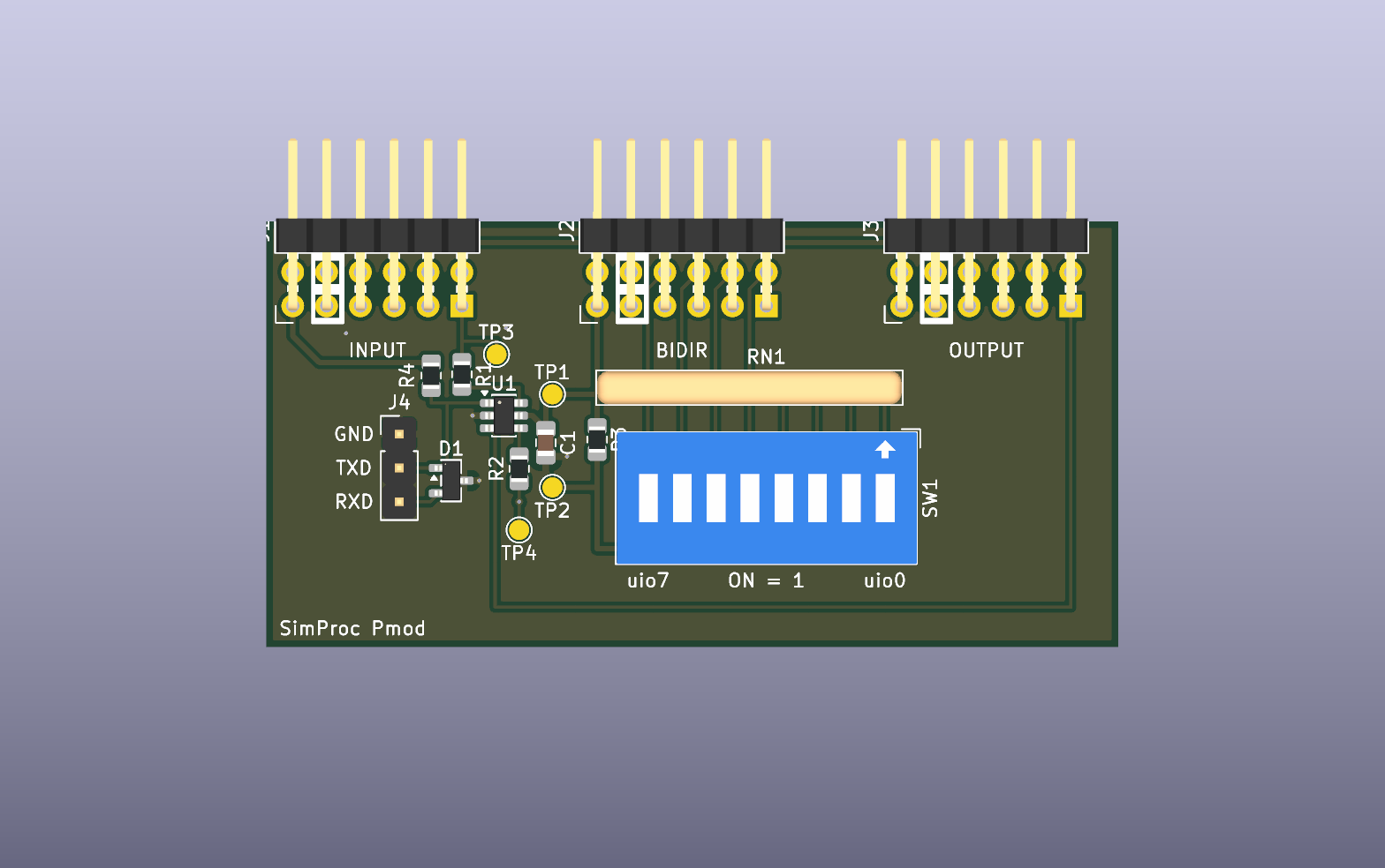
The Brief D reference board from the top Our Brief D board, rendered by
kicad-cli10.0.5 with the parts’ 3D models. It’s Lab 04’s SimProc Pmod with TP3 added to the right of R1, and TP4 below R2.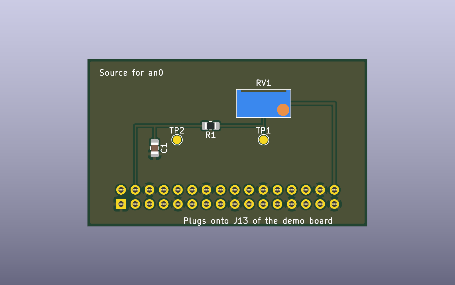
The Brief A reference board from the top Our Brief A board, 50 × 30 mm, seen from the top. J1 runs along the bottom edge on the underside, so only its pads show. RV1 is a 1 kΩ trimmer, R1 and C1 are the filter at the pin, and the track down the left side goes to J1’s pin 4.
Part 3: Decisions and the bring-up plan
Why is each part there, and what will you read at each step?
Write the Decisions in
DESIGN.mdas a numbered list, with one item for each part or choice. Each item gives the value that justifies it, with its unit, and has a line startingMeets:that names the requirements it meets. Every requirement needs at least one decision. Work every number out in the note itself, as our references do. For our R1, the 1 kΩ resistor after the buffer onui[0], that might be “3.3 V × 36 kΩ / 37 kΩ = 3.21 V against the RP2350’s 36 kΩ pull-down, above the 2.31 V the chip needs for a high”, and for the pull-down on Brief A, with a 1.25 kΩ source, “1.25 kΩ / 10 MΩ = 0.0125 %”.For Brief A, take care over the current that the pin’s sampling capacitor draws on average. It’s roughly \(C \cdot V \cdot f_s\), and the voltage it drops across your source’s resistance is an error at the pin. Before you work it out, write down whether you think it matters for an 8-bit converter. Our reference assumes a sample rate of 400 kS/s, because CrossWalk’s documentation doesn’t give one yet. At that rate the current is 5 pF × 3.3 V × 400 kHz = 6.6 µA, and across 1.25 kΩ it drops 8.3 mV, which is 0.64 of one 12.9 mV step. That’s why our trimmer is 1 kΩ and not 10 kΩ.
TipAnswerIt does. With a 10 kΩ trimmer, the source’s resistance can reach a quarter of 10 kΩ, with the wiper in the middle, plus R1’s 1 kΩ: 2.5 kΩ + 1 kΩ = 3.5 kΩ. The same 6.6 µA then drops 23 mV, nearly two steps. The charge that a single sample takes from a 10 nF capacitor is small (5 pF / 10 nF = 0.05 %), but at a high sample rate the capacitor never fully recovers between samples, so the average current decides the error. A buffer amplifier between the trimmer and the filter would make the source’s resistance small, and adding one is the second item under Going further.
Fill in Checks (what you checked and how) and Open questions (what you couldn’t settle, and who could). Our Brief A reference lists four open questions, one of them the DNP mark on J13.
Write
BRINGUP.md. For Brief D, start from your Lab 04 plan and change the steps that measure the UART lines so that they measure at your new test points; in ours, step 6 measures at TP4 and step 7 at TP3. For Brief A, copy Lab 04’s template and fill it in for your board, where the lines that leave the board are the analog pin, 3.3 V and GND. As in Lab 04, every step needs anExpect:with a value and its unit.Commit, and run the check. You should see
ok design ...with your own counts, for example9 requirements, 11 decisions, every requirement met, and for Brief Aok bringup PASS BRINGUP.md: 6 of 6 parts ok.
Part 4: Review it and push
Would your board pass the review you gave the seeded one?
Review your own board against the checklist from Lab 06, line by line, and write what you checked under Checks in
DESIGN.md. Fix what you find. For a line that doesn’t apply, say why, as “there is no IC, so nothing needs decoupling” does in our Brief A note.Commit, push, and wait for your workflow’s run. You should see it green, with the
board-outputsartifact.Run the check one last time on the commit you pushed. You should see every row
okand the last linePASS pmod, Brief D: 5 of 5 capstone checks ok, or for Brief APASS source, Brief A: 8 of 8 capstone checks ok, with your own KiCad project’s name in place ofpmodorsource.
The check can’t tell whether your requirements are the right ones, whether a decision’s reasoning holds, or whether the values in BRINGUP.md are what you’ll read. It takes a person reading DESIGN.md and BRINGUP.md to judge those, and nobody should power a kit with your board on it until someone other than you has read the plan.
Finishing
You’re done when ~/pcb101/labs/capstone-a-board-for-a-team-chip/check.sh --brief D (or --brief A), run in your own repository on the commit you pushed, ends with PASS, and that commit’s run on GitHub is green.
Questions:
Brief D asks for test points on the dongle lines, and not on the project’s clock. Why can’t a Pmod give you a test point on the clock?
TipAnswerThe clock doesn’t come out on the Pmod sockets. On the demo board (
tt-demo-pcbat bbf3dd1), each I/O socket carries eight project pins, GND on pins 5 and 11, and +3V3 on pins 6 and 12, and nothing else. The clock, which the RP2350 usually provides, reaches the chip without passing through any of them. To probe it, use the test point that the breakout has on its clock line.For Brief A, why put a 10 nF capacitor right at the pin? With the source’s largest resistance, 1.25 kΩ, its RC corner is at 12.7 kHz, far above anything a trimmer turned by hand can do.
TipAnswerIt’s there mostly as a reservoir of charge. When the pin’s analog switch closes, the capacitance behind it, up to 5 pF, charges from whatever is closest, and with 10 nF at the pin that charge moves the voltage by only 0.05 %. The capacitor filters as well, so it also keeps noise picked up on the board, and noise from the trimmer’s wiper, out of the pin.
Submit: the URL of your repository and the hash of the commit the check passed on.
Going further (optional)
- Order your board with your cohort, after a second person has read
BRINGUP.md, and bring it up once there’s a chip to bring it up with. Reviewing and ordering a board has the costs. SimProc is on TTSKY25b, so it could be on a bench before the TTSKY26d chips, which are expected in May 2027. - For Brief A, add a buffer between the trimmer and the filter, and work out how much of the sampling droop it removes. If you use KiCad’s
MCP6001R, a 1 MHz op-amp in SOT-23-5, check its supply pins. Its pin 2 is V+ and its pin 5 is V−, the reverse ofMCP6001-OT, which is the plain MCP6001 in the same package. A swap like that, between two variants of one part in the same package, is the kind of fault you looked for in Lab 06. - Do both briefs.
Next on the Course path: this is the last row. A second course, PCB201, would take up what PCB101 left out: 4-layer boards and decoupling for a QFN, characterization boards with a reference of their own, and high-speed signals.