Tiny Tapeout’s boards, part by part
This page answers: what is actually on the boards a Tiny Tapeout chip arrives on, and how do you read a board that someone else designed?
Tiny Tapeout publishes its boards as KiCad projects under the Apache 2.0 licence, so you can open the same files the boards were made from. They’re the best boards to read first, because they were built and shipped, and their files record the decisions a board designer makes for a chip, in KiCad’s own format. The course fetches them from Tiny Tapeout’s repositories at fixed commits, with a script you run in Lab 01, so the boards on this page are the versions you’ll open.
| Board | Repository and folder | Title block | Size | Copper layers | Saved by |
|---|---|---|---|---|---|
| SKY130 QFN breakout | breakout-pcb/breakout-sky-qfn |
rev 3.2, 2025-10-04 | 50 × 50 mm | 4 | KiCad 9 |
| IHP QFN breakout | breakout-pcb/breakout-ihp-qfn |
rev 1.2, 2026-08-18 | 50 × 50 mm | 4 | KiCad 10 |
| Demo board | tt-demo-pcb |
“Tiny Tapeout Demoboard v3”, rev 3.3, 2026-06-23 | 85 × 85 mm | 4 | KiCad 9 |
| DIP dock | breakout-pcb/dip-dock |
rev 1.0, 2026-10-19 | 85 × 85 mm | 2 | KiCad 10 |
The sizes are the extent of each board’s outline, the copper layers are the ones each board file defines, and “saved by” is the generator_version in the board file. breakout-pcb is at commit 91a2bf1 and tt-demo-pcb at bbf3dd1.
The SKY130 QFN breakout
This is the board that carries a SKY130 chip, so most of the team’s chips will arrive on it, and it’s the board you open and read in Lab 01.
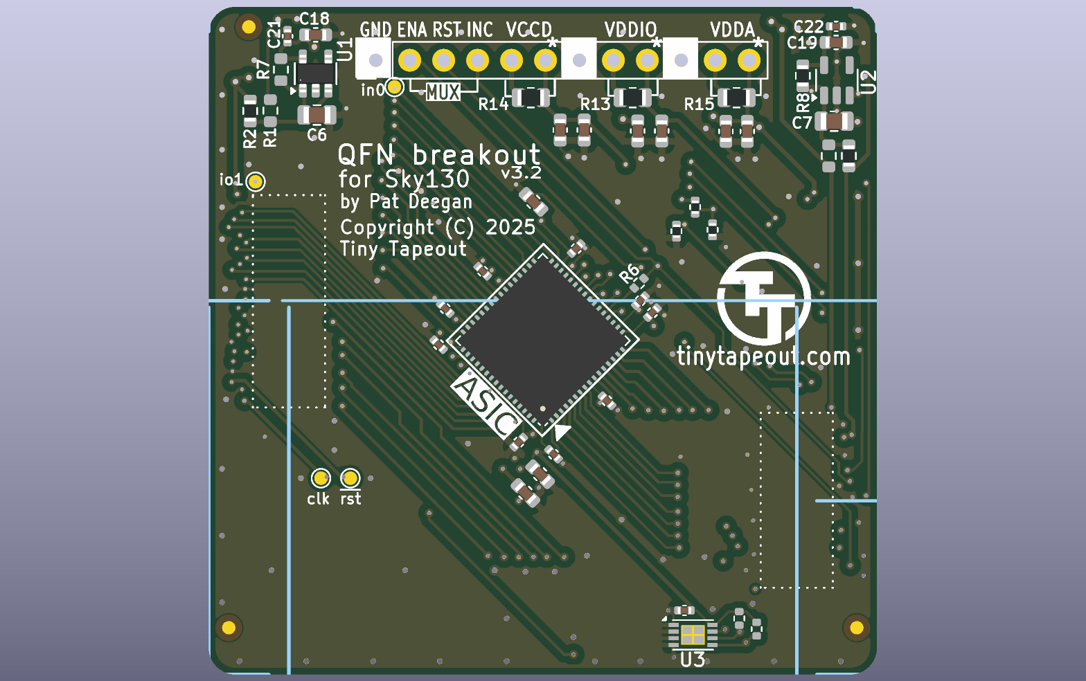
The top of the SKY130 QFN breakout, rendered by kicad-cli 10.0.5 from the board file, with KiCad’s 3D models of the parts. Around the parts, the render shows the board’s own pads, holes and silkscreen, and the copper under the solder mask. kicad-cli pcb render leaves out the models of parts marked DNP, so U2 and U3 show only their pads. Made by scripts/figures/kicad_figures.sh, as are the other renders on this page.
The chip, U4, sits in the middle on KiCad’s own footprint QFN-64-1EP_9x9mm_P0.5mm_EP7.65x7.65mm, which is for a 9 × 9 mm QFN with 64 pins at 0.5 mm pitch and a 7.65 mm square exposed pad underneath. Its schematic symbol, Openframe_QFN_TT06_REV2, comes from Tiny Tapeout’s own library. The chip is placed at 45° to the board’s edges, which the board file records as a rotation of 135°.
Around it are the footprints of the parts that power the chip, and a few others. U1 and U2 are SOT-23-5 footprints for an AP2112K-1.8 regulator. U3 is a footprint for a 24LC02 EEPROM. J2 is the footprint for a 1 × 12 header along the top edge, and the silkscreen labels its pins GND, ENA, RST, INC, VCCD, VDDIO and VDDA. There are also four test points, a set of resistors (several of them 0 Ω), and capacitors in three sizes, 0402, 0603 and 0805. Those are imperial size codes, and KiCad’s footprint names give the metric size as well, so C_0402_1005Metric is for a part 1.0 × 0.5 mm. The schematic explains what the parts are for in notes on the sheet. One reads “For Sky: VCC* 1v8 / VDD* 3v3”, which gives the voltages of the chip’s core supply (VCCD, 1.8 V) and of its I/O and analog supplies (VDD_IO and VDDA, 3.3 V). Another says the “Breakout is fed 3v3 (guaranteed) and 5V (assumes USB supply) and regulates core voltages as needed. Each LDO has jumpers to select source or bypass completely.” A third says that “each supply pin is jumpered and may be monitored or fed through these headers by popping off the relevant resistor (0805s for easier manip)”.
So the board has footprints for more than one way of powering the chip, and a finished breakout is built for one of them. In Lab 01 you list which parts are fitted, and then follow each supply from the connectors to the chip’s pins to find out which way this revision is built.
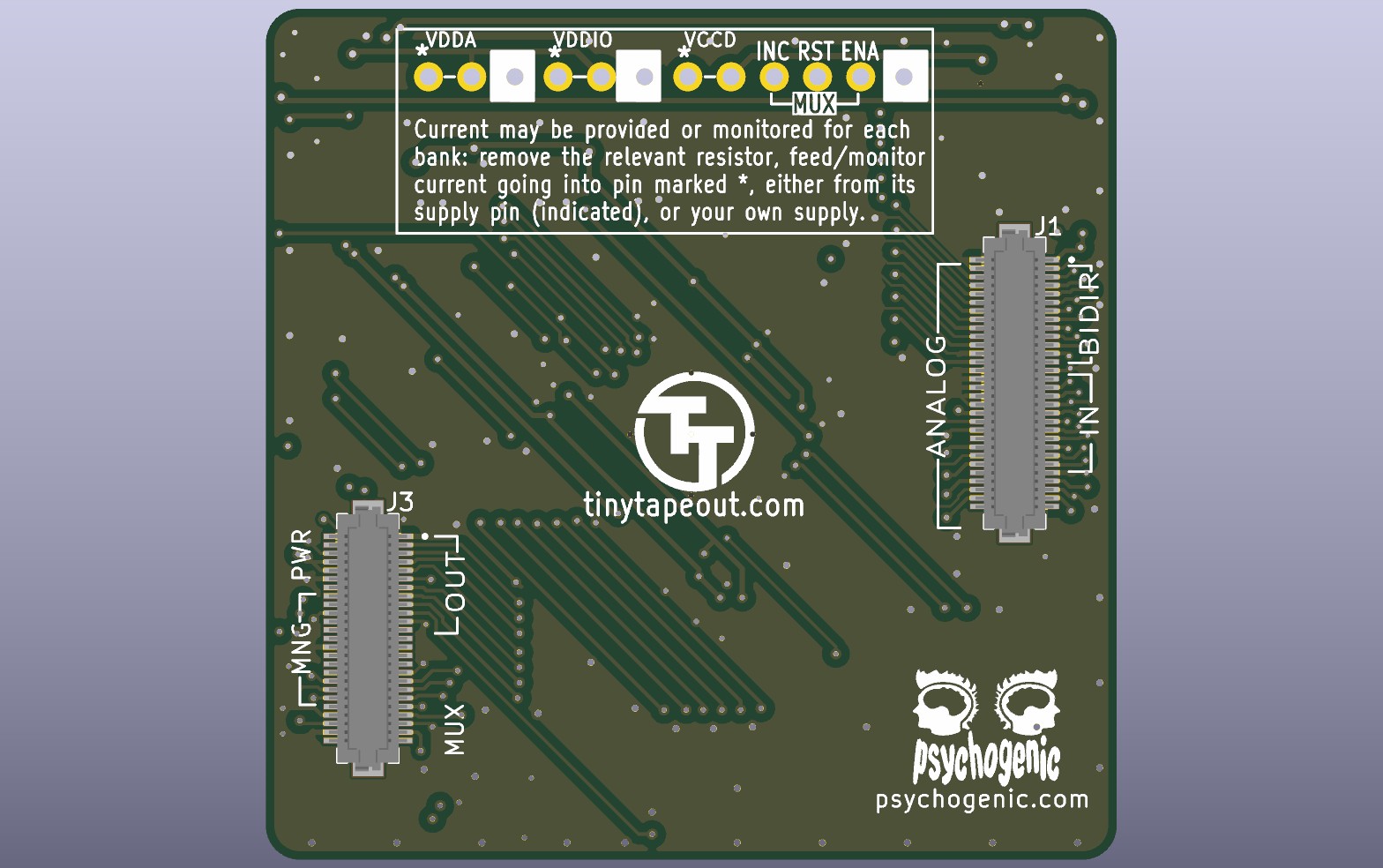
The bottom of the breakout, with its two Hirose DF12 connectors, J1 with 60 pins and J3 with 50. They plug into the demo board and carry every signal and supply between the two boards.
Unfitted footprints and DNP
A footprint on a board means the copper will be there, but not that a part will be fitted to it. When a designer leaves room for a part that a particular build doesn’t use, they mark it DNP in KiCad, for “do not populate”. In the board file a DNP footprint carries dnp in its attributes, and in the schematic its symbol carries (dnp yes) and is drawn crossed out. Several of the breakout’s footprints are marked that way.
DNP affects assembly and not fabrication. The fabricator still makes the pads of a DNP footprint (you can see U2’s and U3’s pads in the render above), and the assembler leaves them empty. kicad-cli, which the course’s checks run, adds a DNP column to a bill of materials by default, and its --exclude-dnp option leaves DNP parts out of a bill of materials or a position file. You make both files in Lab 05.
The board file says what the designer intended. For what was built, Tiny Tapeout keeps a separate repository, pcb-files, which preserves “the PCB/PCBA production files as they were used when creating the relevant run”, including the bill of materials sent to the assembler. In Lab 01 you compare the breakout’s DNP marks with that bill of materials for the same revision.
Links and jumpers
The breakout’s supplies run through 0 Ω resistors, which are parts in an ordinary resistor package whose resistance is (very nearly) zero. A 0 Ω resistor behaves as a wire, but the assembly machine places it like any other resistor, and you can take it off with a soldering iron to open the connection, so it works as a jumper you can change after the board is built. Three of the breakout’s links are larger 0805 parts, “for easier manip” in the note’s words, because those are the ones you’d take off by hand to measure a supply or to feed it from outside.
The demo board puts a second kind of jumper on each of its eight uo_out lines, so every project’s outputs go through one. The net names in its board file give this path from uo_out0:
uo_out0goes to one side of JP2, a two-pad solder jumper whose footprint is bridged with copper (KiCad calls the partSolderJumper_2_Bridged).- The other side of JP2 goes to R19, a 510 Ω resistor in an 0402 package.
- The other side of R19 goes to segment A of the 7-segment display, U4.
uo_out1 takes the same path through JP3 and R20 to segment B, and so on up to uo_out7, which reaches the decimal point through JP9 and R32. A bridged solder jumper is closed as made, and you open it by cutting the thin copper between its pads. So unless someone cuts its jumper, each uo_out pin drives a display segment through 510 Ω, and any load your own board puts on that pin comes on top of the segment.
On the input side, the input DIP switch SW1 has eight switches, and each one that’s on connects its ui_in line to the 3.3 V supply through its own 1 kΩ resistor (R1, and R4 to R10).
The demo board
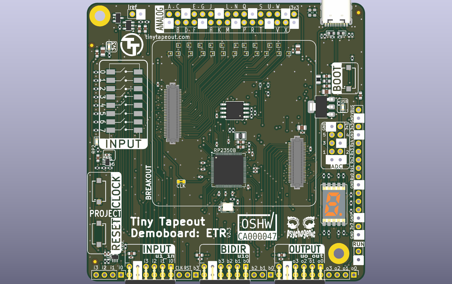
The demo board, rev 3.3, from TinyTapeout/tt-demo-pcb at bbf3dd1. The rectangle marked BREAKOUT is where the breakout plugs in.
The demo board’s microcontroller is an RP2350, U6, in a QFN-80 with 0.4 mm pitch, and its flash memory, U7, is an 8-pin SOIC. A TLV1117LV33 regulator, U1, makes 3.3 V from the USB supply, which comes in on the USB-C connector, J1. Besides the input switches and the display, the board has the unfitted analog header along the top, J13, whose lines are labelled A to X, and the three I/O Pmod sockets along the bottom edge, J14, J15 and J16. In the board file the three Pmod sockets have their pin 1 at x = 92.70, 115.56 and 138.42 mm, 22.86 mm (0.9 in) apart, and a board that plugs into all three has to match that spacing exactly.
The demo board also has 24 TVS diodes, which clamp fast voltage spikes such as an electrostatic discharge. Two of them, D1 and D2 (value “TVS”), are on the USB data lines, and the other 22 (value “5VTVS”, in SOD-882 packages) are on the analog header’s lines /A to /X. None of them is on a digital project pin, so the project pins that a Pmod board reaches have only the chip’s own protection. Supplies, back-powering and ESD covers the ESD protection you add to your own board for them.
The DIP dock
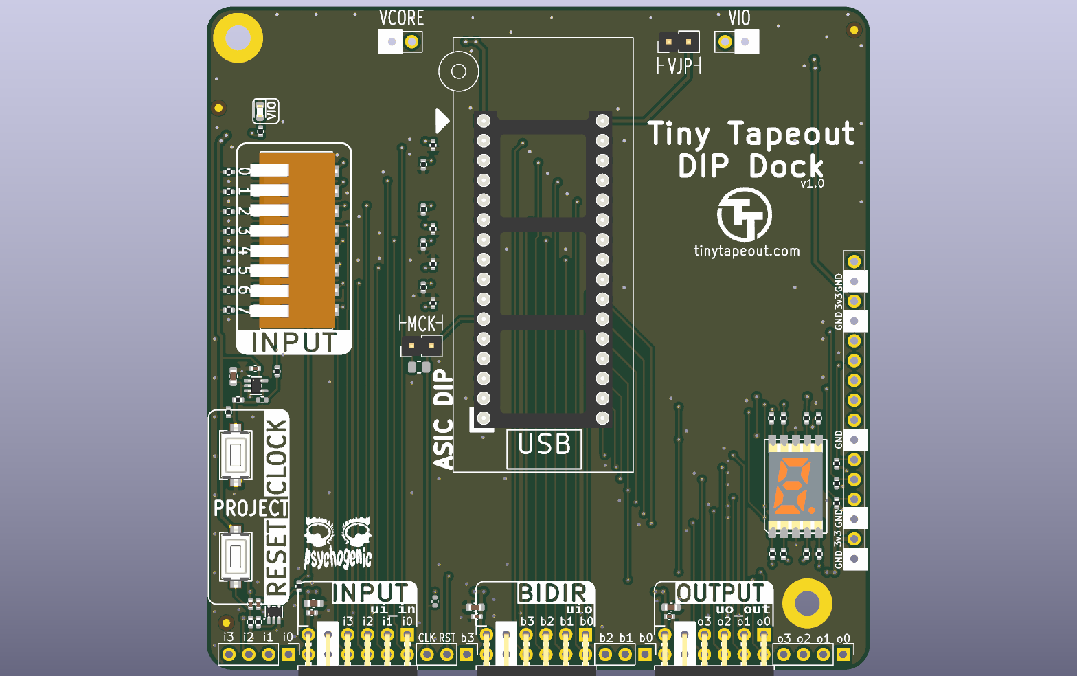
The DIP dock, rev 1.0, from TinyTapeout/breakout-pcb at 91a2bf1.
Not every Tiny Tapeout chip comes in a QFN on a breakout. For chips delivered on a DIP carrier, Tiny Tapeout made the DIP dock. Its README calls it a “Docking station for Tiny Tapeout DIP breakouts” and says it “provides the same footprint, and same interfaces” as the demo board, which it lists as the input DIP switch, the 7-segment display, Pmods for I/O, and manual clock and reset. The README also says “The board is very simple, and designed using only two layers.”
The board file does have two copper layers, and much of it follows the demo board’s file. Its outline is the same 85 × 85 mm, its three Pmod sockets (J5, J6 and J7) sit at the same x = 92.70, 115.56 and 138.42 mm, and its three fiducials (the bare copper dots an assembly machine aligns to) are at the same coordinates. Its custom design rules file, dip-dock.kicad_dru, is an exact copy of the demo board’s, including rules for a QFN-80 and a USB-C connector that the dock doesn’t have. Copying a rules file from an older board is common, and here it does no harm, because a rule that matches no parts checks nothing. Layers and fabricator rules shows a rule on the SKY130 breakout whose condition matches no part on that board either, and explains why you should read the rules you inherit before you rely on them.
Of Tiny Tapeout’s boards, the DIP dock is the most like the board you draw in Lab 03, which also has two layers, the same Pmod spacing and simple parts. The dock’s Pmod sockets are the host side, the side a Pmod plugs into, and your Lab 03 board is the Pmod that plugs into them.
Two layers and four
Three of these four boards have four copper layers, and the DIP dock has two. A 4-layer board’s two extra layers are inside it, between the top and bottom layers. On the SKY130 breakout, a ground zone fills all four layers around the tracks, and the first inner layer is almost solid ground, which gives the signals on the top layer a return path close underneath them. A 2-layer board has to route on both of its layers and fit its ground in around the signals. Layers and fabricator rules shows both stackups from the board files.
Tiny Tapeout’s errata
The breakout-pcb README describes two mistakes in earlier boards. It says the TT07 breakout “has the ASIC project MUX reset_n and increment wires crossed and is thus mislabelled”, and that the production run of the TT06 demo boards “had very low valued resistances which, if you wish to interact with analog projects, had to be removed or replaced.”
KiCad’s checks don’t find mistakes of either kind. ERC checks the schematic against rules about pins, and DRC checks the board against geometric rules and against the schematic. Neither reports two wires that connect cleanly to the wrong pins, or a resistor of the wrong value. You find mistakes like these by reading the board against what it’s meant to do, which is the review you do in Lab 06.
Check yourself
U2 on the breakout carries the
dnpattribute. Does the bare board you’d get from the fabricator have pads for U2?TipAnswerYes. DNP tells the assembler not to fit the part. The footprint’s copper is still part of the board, which is why U2’s pads show in the render.
Why would a designer put a 0 Ω resistor in a supply line instead of a plain track?
TipAnswerSo that the connection can be opened after the board is built, by taking the resistor off. With the link removed you can put a meter in its place to measure the supply’s current, or feed that pin from somewhere else, as the breakout’s notes describe. A track would have to be cut, which is much harder to undo.
You design a board to plug into the demo board’s three I/O Pmods. Will it also plug into the DIP dock?
TipAnswerMechanically, yes: the dock’s three Pmod sockets are at the same positions, 22.86 mm apart, and its README says it provides the same interfaces as the demo board, Pmods for I/O among them.
The TT07 breakout had its
reset_nandincrementwires crossed. Would ERC or DRC have reported it?TipAnswerNo. The wires connected cleanly, just to each other’s pins. ERC and DRC report broken rules, such as unconnected pins, conflicting outputs or copper too close together. Two swapped wires break none of those rules, so it takes a review against what the design is meant to do to catch them.