Symbols, footprints and libraries
This page answers: the schematic shows the chip as a box with 65 pins, and the board shows it as 64 pads around a square. What ties the two together, and where do they come from?
Most parts in a KiCad design are drawn twice. A part’s symbol is what you place in the schematic, and it says what the part does: which pins it has, what they’re called and what kind of pin each one is. Its footprint is what you place on the board, and it says where the copper, solder and markings go. (A few things are drawn only once. A ground symbol has no footprint, and a stitching via on the board has no symbol.) KiCad joins the two through one field on the symbol, which names the footprint, and through the symbol’s pin numbers, each of which has to match a pad number on the footprint. Both drawings come from libraries, which KiCad finds through library tables. This page covers symbols, then footprints, then libraries, with the chip on Tiny Tapeout’s SKY130 breakout as the example throughout, and in Lab 02 you make a symbol and a footprint of your own.
Symbols
A symbol is a drawing with pins. Each pin has a number, a name and an electrical type. The electrical types are what ERC checks, as Schematics other people can read showed. A symbol also has fields: a reference (U4), a value, a footprint, a datasheet link and a description. A part with several identical sections, such as a quad op-amp, can be split into units, each drawn separately.
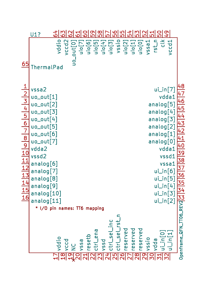
The symbol Openframe_QFN_TT06_REV2 from Tiny Tapeout’s library (tinytapeout-kicad-libs at 0e99691), plotted by kicad-cli 10.0.5. Made by scripts/figures/kicad_figures.sh.
The breakout’s chip uses the symbol Openframe_QFN_TT06_REV2, whose description field reads “Openframe QFN packaging, with TinyTapeout 6+ pin mapping”. It’s a single unit with 65 pins. Pins 1 to 64 are the package’s pins, and pin 65, named ThermalPad, is the exposed pad underneath the package. Of the 65, 19 are power inputs (the supply and ground pins, and the thermal pad), 12 inputs, 11 bidirectional, 10 outputs, 12 passive (the analog pins) and 1 not connected. The symbol’s footprint field already names a footprint, Package_DFN_QFN:QFN-64-1EP_9x9mm_P0.5mm_EP7.65x7.65mm. Every footprint reference has that form: a library’s nickname, a colon, and the footprint’s name in that library.
ERC works from the pin types in the symbol, so a pin drawn with the wrong type can hide a mistake from it. If a supply pin were drawn as passive, ERC couldn’t tell you when the supply was missing, and if two outputs were drawn as bidirectional, it couldn’t tell you when they fought. So when you make a symbol from a datasheet, check the pin types as carefully as the pin numbers.
Footprints and their layers
A footprint is a set of numbered pads plus drawings on the board’s technical layers. The pad numbers join it to the symbol. Symbol pin 17 connects to whatever pad is numbered 17, so the symbol’s pin 65, ThermalPad, connects to the footprint’s pad 65, which is the exposed pad. KiCad checks only that the numbers match, not that a pin and its pad are the same terminal of the package, so a symbol and a footprint made from two different datasheets can disagree without any check reporting it.
These are the layers a footprint draws on, and what each one becomes:
| Layer | What it holds | What it becomes |
|---|---|---|
F.Cu |
the pads’ copper | copper on the board |
F.Mask |
openings in the solder mask, usually over each pad | the parts of the board that aren’t covered by mask |
F.Paste |
openings in the solder paste stencil | where paste is printed before parts are placed |
F.SilkS |
outline and pin 1 marker (KiCad calls this layer F.Silkscreen in its menus) | printed ink on the board |
F.Fab |
the part’s body outline and its reference | assembly drawings, not the board itself |
F.CrtYd |
the courtyard, the area the part and its pads need | nothing on the board; DRC checks that courtyards don’t overlap |
A part on the back of the board uses the B. layers instead. The copper, mask, paste and silkscreen layers go to the fabricator and the assembler, so a mistake on any of them ends up on the real board. The fab and courtyard layers are for people and for DRC.
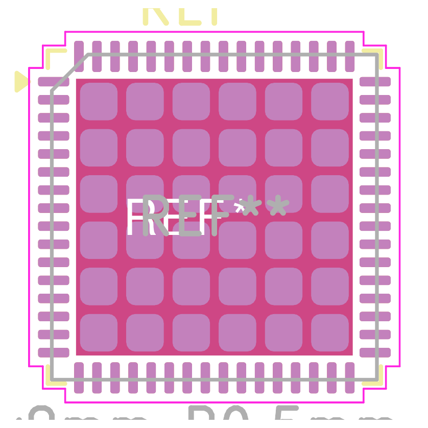
QFN-64-1EP_9x9mm_P0.5mm_EP7.65x7.65mm from KiCad 10.0.5’s Package_DFN_QFN library, with its copper, paste, mask, silkscreen, fab and courtyard layers. Made by scripts/figures/kicad_figures.sh.
The footprint’s 64 signal pads are 0.85 × 0.25 mm rounded rectangles on F.Cu, F.Mask and F.Paste. The exposed pad, pad 65, is a 7.65 mm square on F.Cu and F.Mask only, and its paste is printed through 36 separate 1.03 mm squares in a 6 × 6 grid, which together cover 36 × 1.03² / 7.65² = 65 % of it. KLC’s rule F6.3 says that the exposed pads of large IC packages most often need custom stencil openings like these “to reduce the amount of solderpaste that is applied during stencil application”. The silkscreen lines are 0.12 mm wide, the fab outline is drawn in 0.1 mm lines, and the courtyard is drawn in 0.05 mm lines and reaches 5.13 mm from the centre on each side. From die to package shows where the exposed pad comes from.
KiCad’s library conventions
KiCad’s own libraries follow a set of rules called the KiCad Library Convention (KLC), and the numbers above come from it. Its rules make a good default for footprints of your own. These are the ones you’ll use most, as they read in the KLC’s source at commit 6e8cbad:
| Rule | What it says |
|---|---|
| F4.2 | Pin 1 at the top left (“IPC-7351”); for a QFN with pin 1 in the middle of a side, that side at the top. |
| F5.1 | Silkscreen lines between 0.10 and 0.15 mm, nominally 0.12 mm; no silkscreen over pads, with a recommended 0.2 mm clearance from exposed copper. |
| F5.2 | Fab outline in lines of 0.10 to 0.15 mm (0.10 mm recommended), with a bevel at pin 1 on IC packages. |
| F5.3 | Courtyard in 0.05 mm lines, 0.25 mm clear of the part and its pads by default (0.15 mm for parts smaller than 1.5 mm), 0.5 mm for connectors, crystals and canned capacitors, 1.0 mm for BGAs. |
| F6.3 | Rectangular SMD pads as rounded rectangles; at least 0.2 mm between an exposed pad and the other pads; paste over 50 % to 80 % of an exposed pad’s area, 65 % recommended. |
| F7.5 | Annular ring of a through-hole pad at least 0.15 mm (“IPC-2221”). |
| F7.6 | Finished hole at least the lead’s maximum diameter plus 0.2 mm (“derived from IPC-2222 class 2”). |
KLC is written for a library that has to work for everyone, not for any one fabricator, and a fabricator’s own minimums can be stricter than KLC’s numbers. Of the three fabricators that Layers and fabricator rules compares, JLCPCB asks for silkscreen lines at least 0.15 mm wide and PCBWay for silkscreen characters at least 0.15 mm wide, and KLC’s footprints draw their silkscreen at 0.12 mm. That page also shows what happens when you check a board against a fabricator’s numbers.
Footprints for the same package
The KiCad image that the course’s checks run in has 155 footprint libraries, and Package_DFN_QFN alone holds 776 footprints. Thirty of them have names that start QFN-64-1EP_9x9mm_P0.5mm. They share a 9 × 9 mm body and a 0.5 mm pitch, and they differ in the exposed pad, which comes in 16 sizes from 3.4 mm to 7.65 mm square, and 14 of those sizes come in two versions, one with thermal vias and one without. The name spells out what you need to match: the package, the pin count, 1EP for one exposed pad, the body size, the pitch and the exposed pad’s size.
So it isn’t enough to pick a footprint by its body size and pin count. If you put a QFN-64 package with a 4.7 mm exposed pad on the 7.65 mm footprint, the solder would spread far past the edge of the package’s pad, and a package with a 7.65 mm pad would overhang the pad of a 4.7 mm footprint. Tiny Tapeout’s IHP breakout, for example, uses a footprint from Tiny Tapeout’s own library, QFN-64-1EP_9x9mm_P0.5mm_EP4.7x4.7mm_IHP_C, with 4.7 mm in its name where the SKY130 breakout’s footprint has 7.65 mm. The package drawing in the part’s datasheet tells you which footprint is right, and in Lab 02 you work from one.
Libraries and library tables
A footprint library is a folder whose name ends in .pretty, with one .kicad_mod file per footprint. A symbol library is a single .kicad_sym file. KiCad finds them through library tables, which map a nickname such as Package_DFN_QFN to a path. The global tables (fp-lib-table and sym-lib-table in your KiCad settings) list the libraries every project can use, and KiCad sets them up with its own libraries the first time it runs. A project can also have tables of its own, files with the same names beside its .kicad_pro, which add libraries for that project only.
The breakout has both project tables, and each one adds a library from Tiny Tapeout’s library repository under the nickname TinyTapeout. This is the line in its fp-lib-table:
(lib (name "TinyTapeout")(type "KiCad")(uri "${KIPRJMOD}/../tinytapeout-kicad-libs/footprints/TinyTapeout.pretty")(options "")(descr ""))${KIPRJMOD} is the folder the project is in, so this path means “the folder tinytapeout-kicad-libs beside this project’s folder”. In Tiny Tapeout’s repository that folder is a git submodule, and the course’s fetch script puts the same commit of the library there, so the breakout finds its library when you open it. Because the path starts from ${KIPRJMOD}, it doesn’t depend on where a computer keeps its libraries, and the breakout finds Tiny Tapeout’s library on any computer where that folder sits beside it.
The copies inside a design
Once a part is placed, a KiCad design keeps its own copy of the part’s drawings and no longer depends on the library. The schematic stores each symbol it uses in a section of its own, and the board stores every footprint in full. That’s why the breakout opens even without Tiny Tapeout’s library. It’s also why the Footprint Editor, opened on U4 from the board, says that it’s editing the board’s copy.
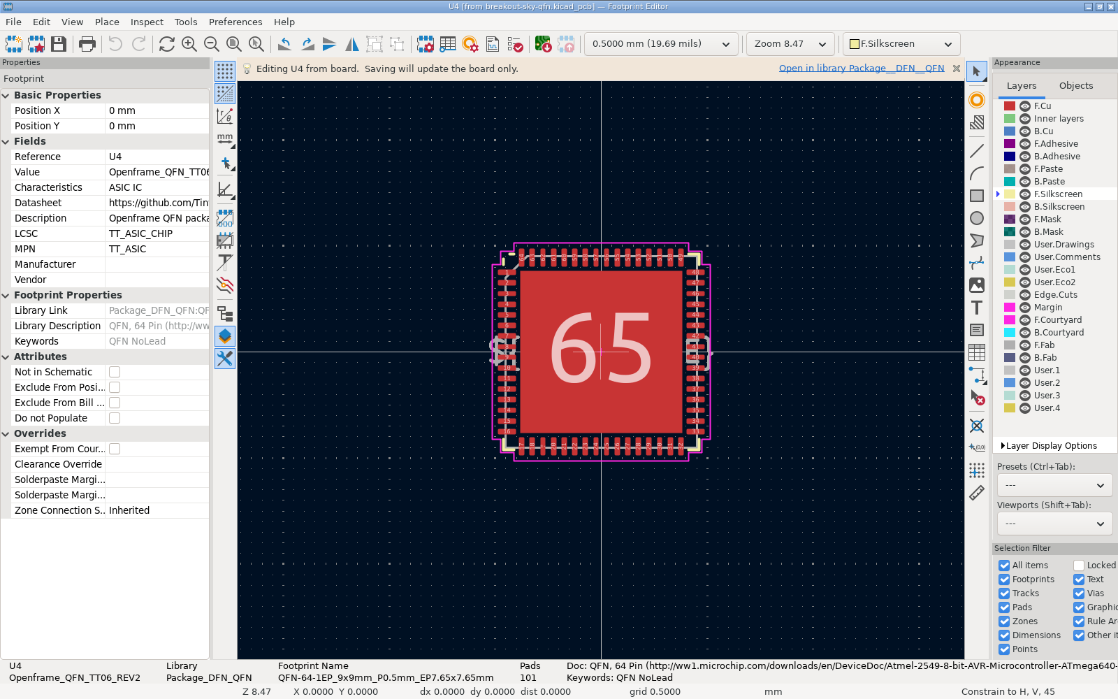
U4 opened from the board in the Footprint Editor of KiCad 10.0.5. The status bar counts 101 pads: 64 signal pads, the exposed pad and its 36 paste openings, which KiCad stores as pads with no copper. Screenshot from scripts/screenshots/kicad/shot.sh.
Keeping copies leads to two kinds of warning. When KiCad can find the library a part came from, it compares the copy with the library’s version, and when they differ it warns. When it can’t find the library at all, it warns about that instead. In the course’s setup, DRC on the breakout reports:
- 44
lib_footprint_mismatchwarnings, such as “Footprint ‘C_0402_1005Metric’ does not match copy in library ‘Capacitor_SMD’”. They cover 25 capacitors, 15 resistors, the two regulators, the header J2 and the chip, whose footprints the board took from KiCad’s own libraries. The three fiducials, the four test points and the EEPROM U3 also came from KiCad’s libraries, but their copies match the library’s, so they get no warning. The warning says that the copies differ, not how. We compared the two versions of U4, and their pads are identical. At the pin 1 corner, the library’s version draws the silkscreen corner mark all the way into the corner and puts a filled triangle beside it, while the board’s copy stops the mark short of the corner and has no triangle. The fields differ as well. - 76
lib_footprint_issueswarnings, all “The current configuration does not include the footprint library …”. 74 are forflyingcarsfootprints, the library that the board’s 73 stitching vias and one of its logos came from, and 2 are forLogos.flyingcarsfootprintsisn’t in either of Tiny Tapeout’s library repositories, so installing Tiny Tapeout’s libraries doesn’t clear these 74.
ERC reports the same two kinds of warning for symbols, 63 lib_symbol_mismatch and 22 lib_symbol_issues. All 63 mismatches are power symbols, such as GND, from KiCad’s power library. Of the 22 issues, 20 are for two libraries that the course’s setup doesn’t have, psycomponents and psypassives, and 2 are for the connectors J1 and J3, because the symbols that the schematic names for them aren’t in Tiny Tapeout’s library. These warnings are about whether the design still matches its libraries, and none of them is about the board’s copper. When a design is a record of a board that was built, its own copies are what was made, so leave them as they are. When you start a board of your own, though, it’s worth resolving them: either update the part from the library, or know why you’ve kept the old copy.
Check yourself
In a symbol you’ve made, pin 17 is
vddio. What connects it to a particular pad on the board?TipAnswerThe symbol’s footprint field picks the footprint, and then pin 17 connects to the pad numbered 17 in that footprint, whatever that pad is. KiCad doesn’t check that pad 17 is really the package’s
vddiolead, so the symbol’s pin numbers and the footprint’s pad numbers have to come from the same package drawing.A friend opens the breakout without Tiny Tapeout’s library beside it. Does the chip’s footprint still appear on the board, and what changes?
TipAnswerIt appears, because the board stores a full copy of every footprint. The warnings change. KiCad can no longer find the
TinyTapeoutlibrary, so ERC reports it missing for the chip’s symbol and for the two connectors, J1 and J3, and DRC reports it missing for the connectors’ footprints. The chip’s own footprint came from KiCad’sPackage_DFN_QFNlibrary, so its DRC warning stays as it was.Your package’s drawing gives a 9 × 9 mm body, 64 pins at 0.5 mm pitch and a 4.7 mm exposed pad. Why is
QFN-64-1EP_9x9mm_P0.5mm_EP7.65x7.65mmthe wrong footprint?TipAnswerIts exposed pad is 7.65 mm square, far larger than the package’s 4.7 mm pad, so its copper and paste would put solder across an area that the package doesn’t cover. Every part of the footprint’s name has to match the drawing, the exposed pad’s size included.
The paste openings on that footprint’s exposed pad cover 65 % of it. What range does KLC allow?
TipAnswer50 % to 80 % of the exposed pad’s area, with 65 % recommended (rule F6.3).
Next: From die to package.