Supplies, back-powering and ESD
This page answers: where does each of the chip’s supplies come from, what happens to the chip when one board is powered and the board connected to it isn’t, and where does static get in?
Protecting the chip’s I/O dealt with each pin on its own. This page starts with the supplies behind the pins. It shows how the breakout makes them, and what SkyWater says about the order in which they come up. Then it follows the current that a powered board can push backwards into an unpowered one, and the current that flows when two boards drive the same line to different levels. Last, it covers static discharge. The demo board has TVS diodes on some of its lines but not on the pins your Pmod reaches, so you put the protection for those pins on your own board.
The chip’s three supplies
The SKY130 chip on Tiny Tapeout’s breakout has three supply rails: VCCD, the 1.8 V core supply; VDD_IO, the supply of the I/O pads; and VDDA, the analog supply. The breakout has footprints for two regulators, and as it’s built only one of them is fitted. Tiny Tapeout’s boards, part by part walks through the whole board, and the figure below shows where each of the three supplies comes from.
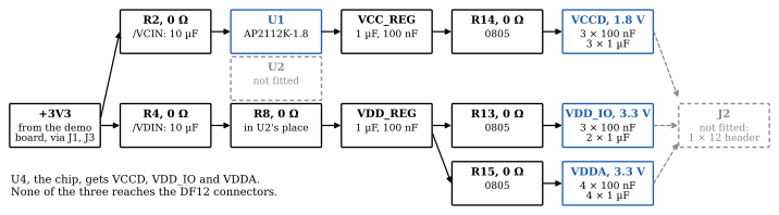
The supplies on Tiny Tapeout’s SKY130 QFN breakout, rev 3.2, as fitted, from the board file at 91a2bf1 (drawn by scripts/figures/sky_breakout_rails.py). U1, an AP2112K-1.8 regulator, makes VCCD. VDD_IO and VDDA come from the demo board’s 3.3 V through four 0 Ω links, with no regulator in between. Both rails go through R4 and then R8, which bypasses the empty footprint of the second regulator, U2. After that, R13 goes to VDD_IO and R15 to VDDA. The dashed parts are marked DNP, for “do not populate”, so they aren’t fitted.
So a board plugged into the demo board can’t set the chip’s supplies one at a time. The only supplies on the breakout’s connectors are +3V3, +5V and ground, so changing +3V3 changes VDD_IO and VDDA together, while VCCD stays at 1.8 V as long as U1 has enough input. VDD_IO is also joined to the demo board’s +3V3 by just three 0 Ω links (R4, R8 and R13), so anything that pushes current into the chip’s I/O supply pushes it into the demo board’s whole 3.3 V net as well.
A regulator and its capacitors
A regulator’s datasheet says which capacitors it needs on its input and output, so U1’s capacitors are part of the regulator’s design. Diodes Inc.’s AP2112 datasheet describes a 600 mA CMOS low-dropout regulator that is “Stable with 1.0µF Flexible Cap: Ceramic, Tantalum and Aluminum Electrolytic”, and it specifies the regulator’s electrical characteristics with 1.0 µF ceramic capacitors on the input and the output. The breakout gives U1 10 µF on its input (C6), and 1 µF and 100 nF on its output (C18 and C21). The six capacitors on VCCD itself come after those, on the far side of R14.
Other regulators are stricter. Horowitz and Hill’s example (The Art of Electronics, 3rd ed., p. 611) is the TPS775xx, whose output capacitor “must be at least 10 µF (with an ESR no less than 50 mΩ and no greater than 1.5 Ω)”, and whose datasheet plots the regions of stability and instability. So when you put a regulator on a board, take the value of its output capacitor from the datasheet, and take its type and series resistance from there too whenever the datasheet sets them, as the TPS775xx’s does.
The order the supplies come up in
We found no required power-up order between VDD_IO, VCCD and VDDA in SkyWater’s user guide for its I/O cells, and no power-sequencing statement from Tiny Tapeout for the chip itself. The guide’s rules are about a supply that is off, and about what the pads do while the supplies come up:
- “no single power supply will be grounded while another supply is active. This will help alleviate the grounded NWELL issues that induce latch-up. It is OK to float a supply while another is active though.”
- Before
vccdis taken to 0 or left floating, the cell’s hold mode must be asserted. - During power-up a control signal,
enable_h, is held low, and “the output driver is forced to a known state (Hi-Z)”.
These rules are written for the people who design the chip’s I/O ring, and the guide says that the chip team is responsible for the levels on those supplies. On the breakout as it’s fitted, VDD_IO and VDDA rise with the demo board’s +3V3, and VCCD follows once U1 has started, so the board fixes the order and nothing on a Pmod can change it.
Back-powering
Tiny Tapeout’s ETR guide uses “back-powered” for feeding the boards 3.3 V on purpose, through a header pin. None of the breakout boards so far needs the 5 V that comes in from USB, it says, so “the boards can be back-powered by feeding 3v3 on a header pin marked as such”. On this page the word means an accident instead, in which a chip is powered through its own input pins.
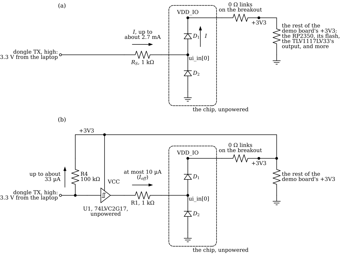
The kit is switched off, but the USB-UART dongle on the SimProc Pmod takes its power from the laptop, and the dongle’s TX line sits high between characters. (a) With only a series resistor \(R_S\) between the dongle and ui_in[0], current flows through \(R_S\) and the pad’s upper protection diode into VDD_IO, and from there through the breakout’s 0 Ω links onto the demo board’s +3V3 net. With 1 kΩ, that’s about 2.7 mA. (b) On Lab 04’s board, the dongle’s TX goes through U1, a 74LVC2G17 buffer powered from the kit’s +3V3, and then through R1 to ui_in[0]. U1 is unpowered too, so at most 10 µA, U1’s \(I_{off}\), reaches ui_in[0]. The pull-up R4 puts up to about 33 µA onto +3V3. Each panel draws the three links as one resistor, and everything else on +3V3 as a second resistor. In the demo board’s file, that net includes its RP2350, the RP2350’s flash memory and the output of its TLV1117LV33 regulator.
Horowitz and Hill say that a HIGH input on an unpowered chip without tolerant inputs will “partially power the supply rail” through the clamp (p. 795). The “craziest” case they give is a CMOS chip whose supply pin was never wired up, and which works anyway because it is “powered by one of its logic inputs (via the chip’s internal input-protection diodes from input to VDD)”, until the moment all of its inputs are low at once (p. 760). Current through those input diodes can also start latch-up (p. 759). Their advice for low-power CMOS boards includes the same warning: “be careful whenever mixing supply voltages. Otherwise you may have current flowing through input-protection diodes” (p. 754).
SkyWater’s rules cover a supply that is grounded and a supply that is floating, and in this case the kit’s +3V3 is neither, because the dongle’s current holds it up at a voltage that depends on that current and on the rail’s load. You can keep that current small, or stop it, in three ways:
- A series resistor on the line limits the current to \((3.3\ \text{V} - 0.6\ \text{V})/R_S\), and keeping it under the 100 µA that SkyWater allows into a pin driven above its supply takes at least 27 kΩ. Protecting the chip’s I/O shows why a resistor that big doesn’t work on
ui_in[0]. The demo board’s firmware turns on the RP2350’s pull-down on that line, and against the strongest pull-down a resistor over 15.4 kΩ leaves the high below the 2.31 V that the chip needs. - A buffer whose inputs accept a voltage even while it’s unpowered sits between the dongle and the chip, powered from the 3.3 V that your Pmod takes from the kit, so when the kit is off, the buffer is off too. In Lab 04 you add a 74LVC2G17, which holds two such buffers, one for each UART line. After each buffer you put a 1 kΩ resistor, R1 on the way into
ui_in[0]and R2 on the way out to the dongle. With its supply at 0 V, TI specifies each of the part’s pins for at most 10 µA (Ioff), so the buffer’s input can take the dongle’s 3.3 V, and its output passes at most 10 µA intoui_in[0], a tenth of SkyWater’s limit. R4, 100 kΩ, holds the buffer’s input high while no dongle is plugged in. With the kit off, it passes up to 3.3 V / 100 kΩ = 33 µA from the dongle into the kit’s +3V3. On the line out of the chip, the dongle’s RX pull-up pushes current into the second buffer’s unpowered output, which passes at most 10 µA.uo_out[0]is on that buffer’s input side, so none of the current reaches it. - A written order for powering and unplugging the boards keeps the dongle from feeding an unpowered kit at all. The buffer already keeps the chip within SkyWater’s limit, so on Lab 04’s board the order is a second protection. It keeps the dongle’s TX off the buffer’s unpowered input and stops the 33 µA through R4. In Lab 04 you’ll write it in
BRINGUP.md, which says which board is powered first and which is unplugged first, and why.
It can also happen the other way round. If the kit is on and the dongle is unplugged from the laptop, the buffer drives SimProc’s TX into the dongle’s unpowered RX input, and current flows through the dongle’s own clamp diode into its supply. R2 limits that current to (3.3 V − 0.6 V) / 1 kΩ = 2.7 mA. None of the dongle datasheets we read gives a limit for it, so allowing 2.7 mA is a judgement of ours. An unpowered dongle may also pull the buffer’s input low through a clamp diode on its own TX pin, and the buffer then holds ui_in[0] low (Protecting the chip’s I/O describes this), so keep the dongle powered whenever it’s plugged into your board.
Contention
Contention means that two outputs are driving one line to different levels at the same time. Only the two drivers’ output resistances limit the current, and it flows for as long as they disagree. A Pmod for a Tiny Tapeout project is never the only thing connected to its pins (Pins, Pmods and planning a pinout has the list), so for each pin you need to know what the other drivers on it are doing:
- The RP2350. The demo board’s firmware has three modes, which the ETR guide’s example
config.inilists:SAFE, with “all RP2 I/O connected pins inputs”;ASIC_RP_CONTROL, in which the “TT inputs,nrst and clock” are driven by the RP2350; andASIC_MANUAL_INPUTS, “basically same as safe, but intent is clear”. The example setsASIC_RP_CONTROLas the default, andconfig.inican set a different mode for each project. A SimProc Pmod drivesui_in[0]from the dongle, through its buffer, so SimProc’s section ofconfig.inihas to selectASIC_MANUAL_INPUTS. On theuiopins, a separate option calleduio_oe_picodecides which of the RP2350’s pins are outputs, and for SimProc it has to leave all eight as inputs, because the switches on your Pmod drive those lines. - The DIP switches. A switch that’s on connects its
ui_inline to +3V3 through 1 kΩ. If your board drives the same line low directly, 3.3 V / 1 kΩ = 3.3 mA flows into your driver, and the line’s low level depends on how stiff that driver is. If your board drives it low through 1 kΩ, as Lab 04’s buffer does through R1, then 3.3 V / 2 kΩ = 1.65 mA flows through the two resistors, and they leave the line at 1.65 V. That’s between the chip’s input thresholds of 0.99 V and 2.31 V (0.3 and 0.7 ×VDD_IO), so the chip can read it either way. For SimProc, switch 1, the one onui_in[0], has to be off. - The chip. On a
uiopin, the project’s ownuio_oedecides whether the chip drives it. SimProc setsuio_oeto 0, so its eightuiopins are inputs and your switches never fight it.
R1 limits a fight on ui_in[0] with a stiff driver, such as the RP2350 in ASIC_RP_CONTROL, so the worst-case contention current is about 3.3 V / 1 kΩ = 3.3 mA. The buffer is a strong driver, rated for 24 mA of output current at 3.3 V, so without R1 only the two output stages would limit the fight.
ESD
Static discharge is another way for current to get into a pin from outside. The human body model, which chip makers test with, treats a charged person as 100 pF in series with 1.5 kΩ, and Horowitz and Hill (p. 804) give its usual charging voltages as 1 to 2.5 kV, with some ICs rated up to 15 kV. At 2.5 kV that’s a peak current of 1.67 A for a pulse with a time constant of 150 ns. Their estimate is that such a discharge delivers 15 µJ to an unprotected input, and that a pair of external clamp diodes, one to the supply and one to ground, with a series resistor on each side of them, cuts that to about 0.1 µJ (p. 805). Ordinary diodes like these have more junction area than the clamps on a chip, so they clamp better. The resistor before them limits the current through the diodes, and the resistor after them limits the current into the chip.
Static gets in wherever something from outside touches the board, such as a connector, a cable or a finger. The demo board’s file has TVS diodes, which are parts made to clamp such pulses, in two places. D1 and D2, valued “TVS”, sit on the USB data lines. Twenty-two more, valued “5VTVS” and in SOD-882 packages (D6 to D27), sit on the lines /A to /X, which run from the breakout’s connector to an unfitted 2 × 16 header. We matched the demo board’s connector to the SKY130 breakout’s pad by pad, and the sixteen digital project lines on that connector all line up. On the breakout, those 22 lines are the analog pads an0 to an11, two res_an lines and eight grounds. The digital project pins have no TVS diodes, so the ui_in, uo_out and uio lines that your Pmod reaches have only the chip’s own protection, and a cable from a dongle gives static a direct path to them. In Lab 04 you’ll put ESD protection on the connector that the dongle’s cable plugs into, from each of its signal pins to ground, so that a discharge arriving on the cable reaches the ESD part before anything else on your board.
Static can also reach the chip while you’re handling the breakout, and each kit has only one chip, so work on an ESD mat, wear a wrist strap, and hold the breakout by its edges.
Check yourself
The kit is off, and the SimProc dongle is plugged into both the laptop and your Pmod. Where does current flow, and what limits it?
TipAnswerOn the board as Lab 03 leaves it, nothing sits between the dongle and the chip. Current flows from the dongle’s TX, which idles high, into
ui_in[0], through the pad’s upper protection diode intoVDD_IO, and through the breakout’s 0 Ω links onto the demo board’s +3V3, where it partly powers everything on that net. Only the dongle’s output stage and the diode’s drop limit it. The dongle’s RX pull-up also pushes current into the unpowereduo_out[0], up to 164 µA for a CH340, one of the chips that dongles use, as Protecting the chip’s I/O works out. On the board as Lab 04 leaves it, the TX drives the unpowered buffer’s input, and at most 10 µA, the buffer’s Ioff, reachesui_in[0]. R4, the pull-up on that input, passes up to 33 µA from the TX into the kit’s +3V3. The dongle’s RX pull-up pushes at most 10 µA into the buffer’s other output, and none of it reachesuo_out[0].Why does SimProc’s section of
config.inineedASIC_MANUAL_INPUTSwhen the Pmod is plugged in?TipAnswerIn
ASIC_RP_CONTROL, the default in the example configuration, the RP2350 drives theui_inpins. The dongle drivesui_in[0]too, through your buffer, so the two would fight.ASIC_MANUAL_INPUTSleaves the RP2350’s pins as inputs.Can a board plugged into the demo board run the chip’s I/O at 1.8 V while
VDDAstays at 3.3 V?TipAnswerNo. The only supplies on the breakout’s connectors are +3V3, +5V and ground, and on the fitted breakout
VDD_IOandVDDAboth come from +3V3 through 0 Ω links. To separate them you’d have to remove R13, the link that feedsVDD_IO, and feedVDD_IOfrom outside through the unfitted header J2.Which lines on the demo board have TVS diodes, and what does that mean for your Pmod’s dongle header?
TipAnswerThe USB data lines, and the lines
/Ato/X, which connect the breakout’s analog pads, and some of its ground pins, to the unfitted analog header. The digital project pins have none, so the dongle header needs its own ESD part, from each of its two signal pins (the dongle’s TXD and RXD) to ground.
Next: Measuring current.