Lab 05: Fab outputs in CI
In this lab you give your board repository a GitHub Actions workflow. On every push it runs ERC, DRC and the schematic parity check on your board. Then it builds the Gerbers and the drill file that a fab needs, the BOM and the position file that an assembler needs, and renders, copper plots and a PDF of the schematic for whoever reviews the board. KiBot then makes an interactive BOM and a design report, and the workflow uploads all of these files as one artifact. You’ll write the .gitignore that keeps KiCad’s local files and the build’s outputs out of git, and finish the commands in the build script that the workflow runs. Then you’ll open the Gerbers in GerbView to see them as the fab will, and write KiBot’s configuration. Last, you’ll break the board on purpose and check that the workflow fails on it.
The lab’s files are in labs/lab-05-fab-outputs-in-ci/ in the course repo.
Before you start
- Finish Lab 04: its check passes on your repository, and the commit it checked is pushed to GitHub.
- Read the pages on row 9 of the course path: Fabrication outputs, Outputs in CI and KiCad files in git.
The check is a bash script, as in Labs 03 and 04, so on Windows you run it in WSL. It runs both KiCad and git inside the course image, and we have run it only on Linux. It also runs KiBot, in KiBot’s own image, which is a 1,347 MB download the first time you run the check.
The lab takes about 1 hour 40 minutes: roughly 10 minutes for Part 1, 10 for Part 2, 25 for Part 3, 10 for Part 4, 25 for Part 5 and 20 for Part 6. Those times are our estimates. We did time the check itself. With one CPU for each container, it took 26 s on our reference repository, and 42 s with --planted, because that also runs the board check on a second commit.
Part 1: Add the workflow
Copy the starter into your board repository and see what arrived:
cd ~/simproc-pmod
cp -r ~/pcb101/labs/lab-05-fab-outputs-in-ci/starter/. .
git status
You should see
git statuslist two new folders,.github/andci/, and alsopmod.kicad_prl, which is still untracked because Lab 03 had you leave it out of your commits..github/workflows/board.ymlis the workflow, andci/build.shis the script it runs.ci/check_board.pyis a copy of the course’s board check.ci/kicad-image.txtnames the pinned KiCad image by its digest, andci/kibot-image.txtdoes the same for KiBot’s image.ci/board.kibot.yamlis KiBot’s configuration, which you’ll finish in Part 5.Read
board.yml. After checking out your commit, it pulls the image named inci/kicad-image.txt, then runsbash ci/build.sh check,fabandimagesas three steps, each in a fresh container. A fourth step pulls the KiBot image named inci/kibot-image.txtand runsbash ci/build.sh kibotin it, and the last step uploads the folderout/as an artifact calledboard-outputs. Then readci/build.sh, which has the commands that those four steps run.Why does the workflow start the containers with
docker runas the runner’s own uid, rather than running the whole job in the image with GitHub’scontainer:setting?TipAnswerSo that the checks run the way the course’s own checks do, as an ordinary uid, with KiCad’s default library tables copied into an empty home folder.
build.shcopies the tables before it runs any stage. A jobcontainer:runs as the image’s own user unless you override it, and wafer.space’s workflow overrides it with--user root. Outputs in CI shows that root in this image has no library tables, so its warning counts differ from the course’s. The course’s ownlabs.ymlworkflow also starts its containers withdocker run, throughkicad.sh, for the same reason.Commit the starter, but don’t push it yet. Name its two folders in
git add, so thatpmod.kicad_prlstays out of the commit:git add .github ci git commit -m "Lab 05 starter"If you pushed it now, would the run on GitHub be green or red?
TipAnswerIt would be green. A step fails only when its command exits with a status other than 0, and the TODOs are comments, so every stage of
build.shsucceeds. KiBot finds no outputs listed inci/board.kibot.yamland exits 0 as well. The artifact has no drill file, BOM, position file, renders, copper plots or KiBot outputs in it, which is why the lab’s check looks at the files the build made as well as at its exit status.build.shhas five TODOs, which you’ll do in Part 3, andci/board.kibot.yamlhas three, which you’ll do in Part 5. There’s no.gitignoreyet either. Before you run anything, write down which rows of the Lab 05 check you expect to fail. Then run it:~/pcb101/labs/lab-05-fab-outputs-in-ci/check.shIt first runs
bash ci/build.sh allin the pinned KiCad image and prints that command’s output, apart from the renders’ progress lines. If the build passes, it runsbash ci/build.sh kibotin the KiBot image, as your workflow would. Either way, it then prints one row per check. On Lab 04’s reference board with the starter copied in and committed, the rows were:ok workflow .github/workflows/board.yml runs check, fab and images in kicad/kicad:10.0.5 and kibot in kicad10_auto_full:1.9.1-2_k10.0.5_d13.2_b4.2.4LTS, both by digest, and uploads out/ ok check the board check passes ok gerbers 9 Gerbers and pmod-job.gbrjob in out/fab/ FAIL drill no drill file (.drl) in out/fab/ FAIL bom no BOM in out/assembly/ (a .csv with 'bom' in its name) FAIL position no position file in out/assembly/ (a .csv with 'pos' in its name) FAIL images out/review/ is missing top render, bottom render, F.Cu plot, B.Cu plot FAIL ibom no interactive HTML BOM in out/kibot/ (the .html that an ibom output writes) FAIL report no design report in out/kibot/ (a .txt from a report output, with a 'Board size:' line) FAIL gitignore no .gitignore; after the build git sees 15 untracked files: out/fab/pmod-B_Cu.gbr, out/fab/pmod-B_Mask.gbr, out/fab/pmod-B_Paste.gbr, out/fab/pmod-B_Silkscreen.gbr ... FAIL pmod: 3 of 10 Lab 05 checks ok; add --planted REV once you've done Part 6
Part 2: Keep KiCad’s own files out of git
Which files in your repository’s folder belong in git, and which should git ignore?
Run
git statusagain. It listsout/, which the build just wrote, andpmod.kicad_prl, whichkicad-cliwrites next to any project it reads. If you’ve saved the board in KiCad, it may also list a.history/folder or apmod-backups/folder, and while the board is open in KiCad, it lists lock files ending in.lck. KiCad files in git says what each one is.Make a
.gitignorein the repository’s root folder. Start from Tiny Tapeout’s, which KiCad files in git prints in full, and add the two lines it doesn’t have:.history/for KiCad 10’s local history, andout/for everythingbuild.shwrites. CI makesout/again on every run, so it never needs to be in git.Run
git status. You should see.gitignoreas the only new file, apart from any files of your own that you haven’t committed yet. If a file you meant to ignore still shows as modified, git is already tracking it. Rungit rm --cachedon it and commit, and git stops tracking it.Tiny Tapeout’s demo board repository lists
fp-info-cachein its.gitignore, and git still tracks the file. How?TipAnswerThe cache was committed four minutes before the
.gitignorethat lists it, and a.gitignoreonly stops git from adding files; it doesn’t affect a file git already tracks. Removing it from the index withgit rm --cached fp-info-cacheand committing would let the ignore rule apply.Commit the
.gitignoreand run the check. You should seeok gitignore nothing untracked after the build, and none of KiCad's local files tracked.
Part 3: Finish the fabrication files and review images
What do a fab, an assembler and a reviewer each need from your CI?
Write the five commands that the TODOs in
ci/build.shask for. Eachkicad-clicommand prints its own options with--help; for example, run~/pcb101/labs/common/kicad.sh kicad-cli pcb export drill --helpand the same for
sch export bom,pcb export pos,pcb renderandpcb export svg. Keep the file names that the comments give, because the check finds each file by its name. Things to decide as you go:- The drill file has to use the same origin as the Gerbers. To see which origin the Gerbers use, open File > Plot in the PCB Editor. If “Use drill/place file origin” isn’t ticked, the Gerbers use the absolute origin, and so should the drill file (
--drill-origin). On our board the drill/place origin was never moved from (0, 0), soabsoluteandplotwrote the same file. On a board where someone has placed that origin, such as the DIP dock, the two options put the holes in different places. - An assembler wants the position file as CSV, in millimetres (
--format,--units), but by default the command writes a text table in inches. - A render takes
--side topor--side bottom. - For the copper plots,
--layers F.Cu,B.Cuwith--mode-multiwrites one SVG per layer,--common-layers Edge.Cutsadds the outline to each, and--page-size-mode 2with--exclude-drawing-sheetcrops them to the board.
- The drill file has to use the same origin as the Gerbers. To see which origin the Gerbers use, open File > Plot in the PCB Editor. If “Use drill/place file origin” isn’t ticked, the Gerbers use the absolute origin, and so should the drill file (
Before you run the check, count the holes that your drill file should have, one for every pad with a hole and one for every via, and write the number down. On our board it’s 70: 36 pins in the three Pmod connectors, 3 in the dongle header, 16 in the switch, 9 in the resistor network and 6 vias.
Run the check. You should see every row
okexceptibomandreport, which fail until you’ve done Part 5. Our rows were:ok workflow .github/workflows/board.yml runs check, fab and images in kicad/kicad:10.0.5 and kibot in kicad10_auto_full:1.9.1-2_k10.0.5_d13.2_b4.2.4LTS, both by digest, and uploads out/ ok check the board check passes ok gerbers 9 Gerbers and pmod-job.gbrjob in out/fab/ ok drill pmod.drl: 70 holes, all inside the outline ok bom pmod-bom.csv: 15 rows, every footprint listed ok position pmod-pos.csv: 13 parts, in mm, where the board has them ok images 5 files in out/review/: renders, copper plots and the schematic FAIL ibom no interactive HTML BOM in out/kibot/ (the .html that an ibom output writes) FAIL report no design report in out/kibot/ (a .txt from a report output, with a 'Board size:' line) ok gitignore nothing untracked after the build, and none of KiCad's local files tracked FAIL pmod: 8 of 10 Lab 05 checks ok; add --planted REV once you've done Part 6The drill row checks that every hole lies inside the outline in the Edge.Cuts Gerber, so a drill file made in a different origin from the Gerbers fails it. Fabrication outputs shows that mistake on the DIP dock.
Our BOM has 15 rows and our position file only 13 parts. Open
out/assembly/and find the two parts that the position file leaves out. Why would KiCad leave them out?TipAnswerThey’re the test points, TP1 and TP2. Their footprint,
TestPoint_Pad_D1.5mm, is a bare pad with nothing to place on it, and it carries the attribute “Exclude from position files” (exclude_from_pos_filesin the board file), so the pick-and-place file skips it. The BOM comes from the schematic and lists them anyway.Commit and push. On your repository’s page on GitHub, the Actions tab shows a run of the workflow, which is named Board, for your commit. The run’s page lists the job’s steps, and once the run has finished, it also has the
board-outputsartifact, which downloads as a zip ofout/. You should see a green run, even though KiBot has nothing to make yet. We couldn’t push from the machine we wrote the course on, so we ran the workflow’s steps locally withsrc/run_workflow.py, with each container limited to one CPU. All seven steps succeeded in 35 s, and the artifact held 21 files. On GitHub the run also has to pull the two images (808 MB and 1,347 MB), which adds to that time, and we haven’t timed a run there.
Part 4: Look at what the fab will get
Do the files CI built describe your board?
Unzip the artifact, open GerbView (the Gerber Viewer, from KiCad’s project manager), and use File > Open Gerber Plot File(s)… for every
.gbrinfab/, then File > Open Excellon Drill File(s)… for the.drl. Theout/fab/folder that the check wrote on your own machine has the same files.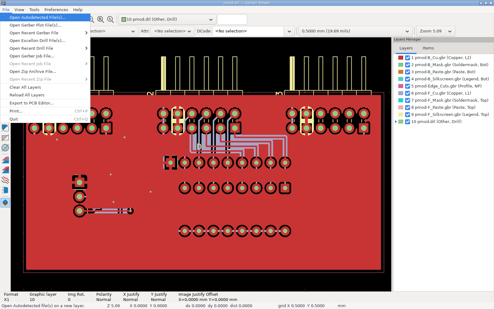
GerbView with its File menu open over the SimProc Pmod’s Gerbers GerbView’s File menu in KiCad 10.0.5, over the nine Gerbers and the drill file that
ci/build.sh fabwrote for our Lab 04 board. We opened these from the command line (gerbview out/fab/*.gbr out/fab/*.drl), which also works if KiCad’s programs are on your path.Before you look closely, write down how many layers the Layers Manager should list and what function GerbView should give each.
Compare the view with your board in the PCB Editor. You should see every drill hit (the small dots of the drill layer) in the middle of its pad, and the Layers Manager listing every file with the function that GerbView read from it, such as “Copper, L1” for the top copper and “Profile, NP” for the outline:
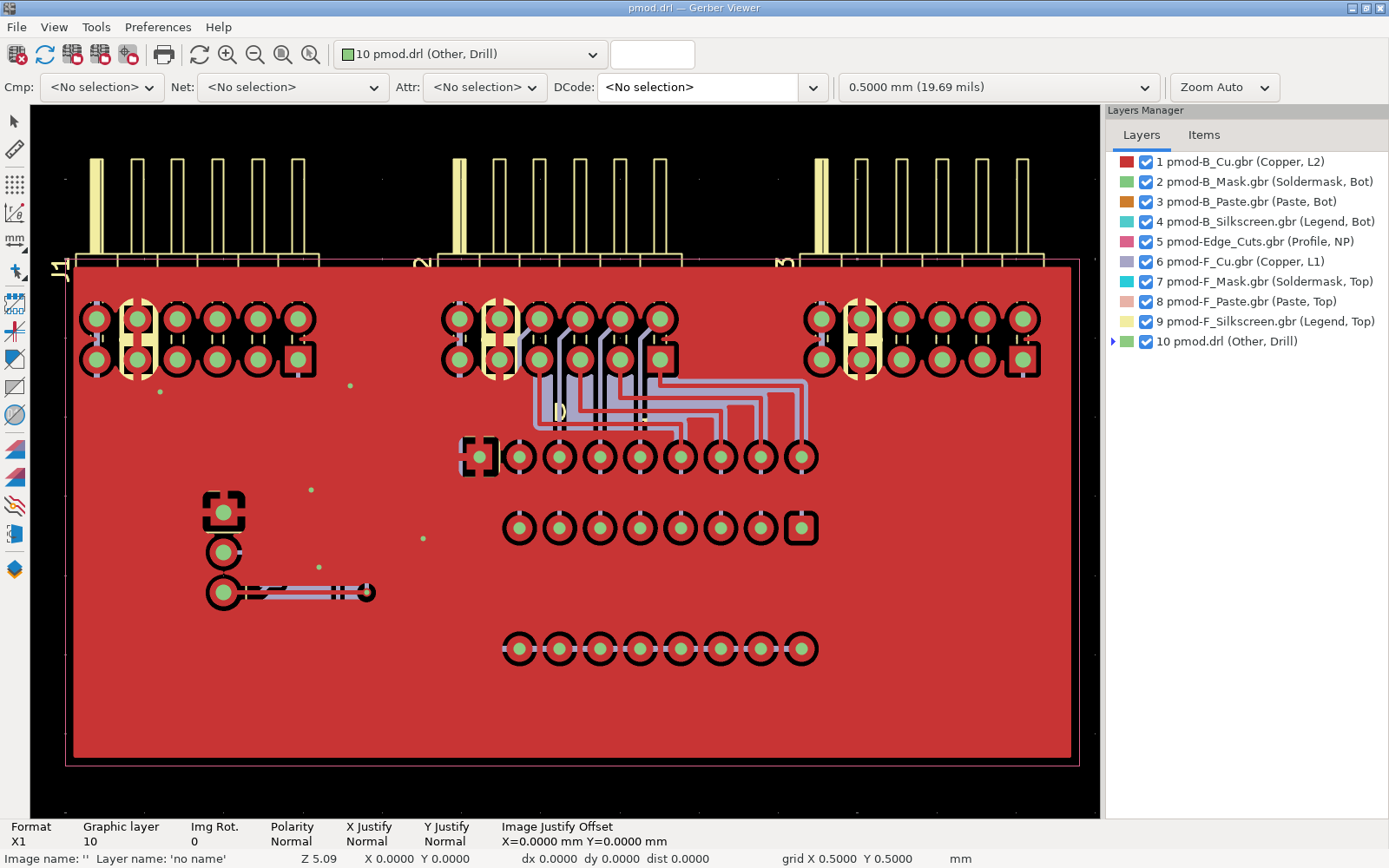
GerbView with the SimProc Pmod’s nine Gerbers and drill file Our board’s nine Gerbers and its drill file in GerbView. The red is the bottom copper, mostly its ground pour, and the lighter tracks are on the top copper; untick a layer in the Layers Manager to see the others more clearly.
If every hole sat the same distance away from its pad, what would you change?
TipAnswerYou’d change the drill file’s origin. The drill file and the Gerbers line up only through their coordinates. If the board’s plot settings use the drill/place origin, the drill file needs
--drill-origin plot, and if they don’t, it needsabsolute. Fabrication outputs shows this offset on the DIP dock.
Part 5: Add KiBot’s outputs
How do you add outputs that kicad-cli can’t make, such as an interactive BOM, and keep the whole run on one version of KiCad?
Look at what the starter put in place for KiBot. KiBot is a program that drives KiCad from a YAML file, and it can make outputs that
kicad-clican’t. It’s free software, under the AGPL-3.0. It needs a good deal of software besides KiCad, so it runs in an image of its own,ghcr.io/inti-cmnb/kicad10_auto_full, whichci/kibot-image.txtnames by its digest. That image carries KiBot 1.9.1 and KiCad 10.0.5, the same KiCad version that the course’s checks use. The workflow’s “KiBot outputs” step pulls the image and runsbash ci/build.sh kibotin it withdocker run, as the steps before it run theirs. KiBot also has a GitHub Action of its own, but the action builds its image from a tag that moves with every KiBot release, so the workflow doesn’t use it (Outputs in CI has the details). Thekibotstage at the end ofbuild.shruns KiBot onci/board.kibot.yamland has it write what it makes intoout/kibot/. You’ll finish that configuration file in step 4.KiBot can also run ERC and DRC itself; it calls them preflights. Why does the workflow keep its checks in
check_board.py, in KiCad’s own image, and use KiBot only for outputs?TipAnswerBecause KiBot’s DRC, with its default settings, doesn’t fail on everything that
check_board.pyfails on, and because its KiCad is a different build. We tried KiBot’s checks on Lab 04’s reference board throughkibot.sh. Witherc: trueanddrc: trueunderpreflight:, KiBot fails only on errors, but KiCad reports a missing footprint as a parity warning. With R3 deleted from the board, KiBot printedWARNING:(W145) (missing_footprint) Missing footprint R3 (10)and exited 0, which is the green run that Outputs in CI warns about. With itswarnings_as_errors: trueoption it fails on every warning instead, and the unchanged board failed on its 32 silkscreen warnings (DRC warnings: 32, promoted as errors, exit status 5).check_board.pyfailed the board without R3 (FAIL parity.warning: 1 (want 0)) and passed the unchanged one. KiBot’sfiltersoption can turn chosen kinds of warning into errors, one kind at a time, so you could make KiBot fail on nearly the same things, but the course would then have two definitions of a passing board to keep in step.The other reason is that KiBot’s image carries KiCad’s Ubuntu build of 10.0.5, with the 10.0.4 symbol and footprint libraries, and warning counts depend on the libraries. Every count on the course’s pages comes from
kicad/kicad:10.0.5, so the check that passes or fails a board stays in that image, and KiBot’s step runs only after it has passed.See what KiBot can make by running its help in KiBot’s image, through the course’s
kibot.sh:~/pcb101/labs/common/kibot.sh kibot --help-list-outputs ~/pcb101/labs/common/kibot.sh kibot --help-output ibomThe first lists 56 types of output. Many of them are files that
kicad-climakes too, such as Gerbers, drill files and position files. Two thatkicad-clidoesn’t make areibom, an interactive HTML BOM, andreport, a design report written for whoever orders the board.kicad-cli pcb export statswrites a board statistics report that overlaps with KiBot’sreport. It gives each hole at its finished size, though, and it leaves out what KiBot adds for the fab, such as the drill sizes, a Eurocircuits board class and an estimate of the solder paste. The second command prints every option of theibomoutput, andkibot --help-output reportandkibot --help-filtersdo the same for the report and for KiBot’s filters.Before you change the configuration, write down which of your board’s parts the interactive BOM should list, and how many rows it will have if parts with the same value and footprint share a row. Then decide what it should do with a part marked DNP (Tiny Tapeout’s boards, part by part explains the mark): should a part you won’t fit be on the list you solder from?
Finish the three TODOs in
ci/board.kibot.yaml. Things to decide as you go:- A filter goes in a
filters:list, with anameof your choosing and atype. Thegenerictype has an option that picks out the parts KiCad marks “Do not populate”;kibot --help-filterslists it. - The
ibomoutput names that filter in itsdnf_filteroption (DNF is “do not fit”), and every part the filter picks out is then left off the BOM. Without a filter, the ibom lists a DNP part along with all the others. - The
reportoutput needs only itsnameandtype. Keep its default template, because the check reads the board size and the drill tools from it. - Leave the file names as KiBot makes them, which for our board were
pmod-ibom.htmlandpmod-report.txt.
- A filter goes in a
Run the KiBot stage in the pinned KiBot image:
~/pcb101/labs/common/kibot.sh bash ci/build.sh kibotYou should see a line for each output, and the two files in
out/kibot/. Ours took 2.3 s with one CPU:pcb101: KiBot image ghcr.io/inti-cmnb/kicad10_auto_full@sha256:96e75f885b15617c6b38aef11db7856a93f4367cab7a0b6c2b30465557619330 == KiBot outputs CI/CD environment detected WARNING:(W182) No instance for `/00000000-0000-0000-0000-000000000000` using the first (kibot - v6_sch.py:1458) - 'Interactive HTML BOM' (ibom) [ibom] WARNING:(W013) U1 not linked to an existing schematic component, but U1 found in schematic, assuming this is the same (kibot - kiplot.py:488) - 'Design report' (report) [report] Found 2 unique warning/s (47 total, 3 filtered)The text in quotes on each output’s line is that output’s
comment. Our configuration gives each output one (Interactive HTML BOMandDesign report). An output without a comment makes the same file, and its line reads- '' (ibom) [ibom].The first warning, W182, comes from the way KiBot reads a schematic. KiBot looks for each symbol’s instance under a sheet path of zeros, while our schematic records each one under the schematic’s own UUID, so KiBot falls back to the symbol’s first instance, as the message says. Our schematic is one sheet, and each of its 43 symbols (the power symbols and U1’s three units among them) has only one instance, so the first instance is the right one. KiBot prints W182 once and counts it for each symbol.
The second warning, W013, is about U1, the 74LVC2G17 dual buffer. The schematic draws it as three units, one for each buffer and one for the GND and VCC pins. Each unit is a symbol of its own in the schematic, with its own UUID. KiBot folds the three into one U1 and keeps the UUID of the first unit it reads, unit 2, which is one of the buffers. Our board’s U1 footprint records the UUID of unit 3, the one with the power pins, so KiBot can’t match the footprint to its symbol by UUID. It looks the footprint up by its reference instead and finds the U1 it folded, which is the right part.
Open
out/kibot/pmod-ibom.htmlin a browser. When you click a row of the BOM, its parts light up on the drawing of the board. You should see the parts and rows that you wrote down in step 3. Ours has 15 parts in 11 rows: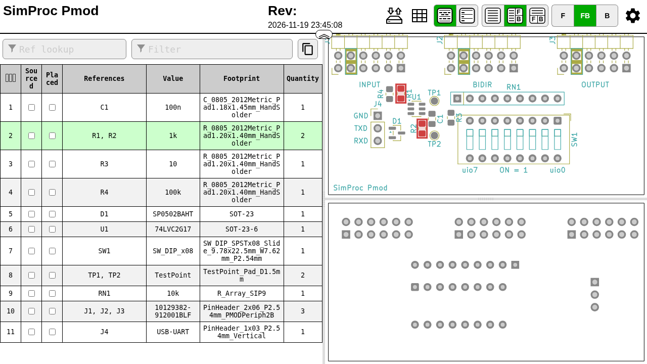
KiBot’s interactive BOM for the SimProc Pmod, with the row for R1 and R2 selected and both resistors highlighted on the front of the board KiBot’s interactive BOM for our Lab 04 board, with the row of the two 1k resistors selected, so R1 and R2 are drawn in red on the front of the board (top right); the bottom is below it. The Sourced and Placed columns are checkboxes to tick as you buy and solder each row, and the page keeps the ticks in your browser’s storage. Made by
scripts/screenshots/browser/ibom.cjs.Our board has no DNP part, so the filter changes nothing on it. What would the BOM have shown for a DNP part without the filter?
TipAnswerIt would have listed the part like any other. The course’s self-test marks J4 DNP in our schematic and on our board, and runs the check twice. With
dnf_filternaming the filter, the ibom listed 14 parts in 10 rows and left J4 out. With that line taken out, it listed J4 again, and the check’sibomrow failed withpmod-ibom.html lists J4, which the board marks Do not populate; give the ibom output a filter for DNP parts (dnf_filter). The BOM thatkicad-climade from the schematic listed all 15 parts both times.Open
out/kibot/pmod-report.txt. It’s plain text, and it gives the board’s size and layers, the sizes that a fab’s rules are about (clearance, track width, drills, vias and annular ring), the holes, and an estimate of the solder paste. Compare its holes with the count that you wrote down in Part 3, step 2. Ours lists three drill tools:Drill tools (including vias and computing adjusts and rounding): - 0.4 mm (16 mils) (6) - 0.9 mm (35 mils) (25) - 1.1 mm (43 mils) (39)That’s 70 holes, as in the drill file, but the vias and the pads on our board have holes of 0.3, 0.8 and 1.0 mm. Why is each tool 0.1 mm larger?
TipAnswerThey’re the sizes of the drills rather than of the finished holes. Copper is plated onto the wall of a plated hole after it’s drilled, which makes the hole smaller, so the drill has to be larger than the hole in the footprint. KiBot allows 0.1 mm for that on every plated hole, and the report says so under “Important sizes”: “The above values are real drill sizes, they add 0.1 mm (4 mils) to plated holes (PTH)”. Every hole on our board is plated, so all three tools are 0.1 mm larger than the holes.
Some lines of the report are KiBot’s defaults rather than facts about your board. Our board file records no stack-up, so the finish (HAL), the material (FR4) and the colours of the solder mask and silkscreen are KiBot’s defaults. So is the “yes” after micro vias and buried/blind vias, which says what KiBot assumes the rules allow; the “Total” line under them counts the vias the board really has. Check those lines against what you’ll order before you hand the report to anyone.
Run the Lab 05 check. You should see the two new rows
ok:ok ibom pmod-ibom.html: 15 parts in 11 rows, none of them marked DNP ok report pmod-report.txt: 64 x 32 mm and 70 holes, as in the Gerbers and pmod.drland the last line
PASS pmod: 10 of 10 Lab 05 checks ok; add --planted REV once you've done Part 6. Theibomrow reads the board data inside the page and compares its BOM with the footprints on your board. It passes when every part that belongs in a BOM is listed, none of the listed parts is marked DNP, and the BOM has nothing that isn’t on the board. Thereportrow compares the report’s board size with the outline in the Gerbers, and checks that its drill tools add up to the number of holes in the drill file. Then commitci/board.kibot.yamland push. The run’s “KiBot outputs” step now makes the two files, and the artifact has akibot/folder. Our local run of the workflow, with one CPU for each container, succeeded in all seven steps in 30 s, and the artifact held 23 files.
Part 6: Break it on purpose
Does your workflow stop a broken board before it makes a set of Gerbers?
You’re about to move a track so that it passes too close to a pad of another net. Write down which step of the workflow will fail, which steps will run after it, and what the artifact will hold.
In the PCB Editor, select a track and drag it (press D) until it passes within 0.2 mm of a pad or track on another net, without touching it. Save. On our board we dragged the 0.4 mm +3V3 track that runs along the top edge from J1 to J2 down by 1 mm, which takes its lower edge to 0.16 mm from the upper row of J1’s pads.
Run DRC in the editor (Inspect > Design Rules Checker, then Run DRC). You should see at least one error. Ours had two:
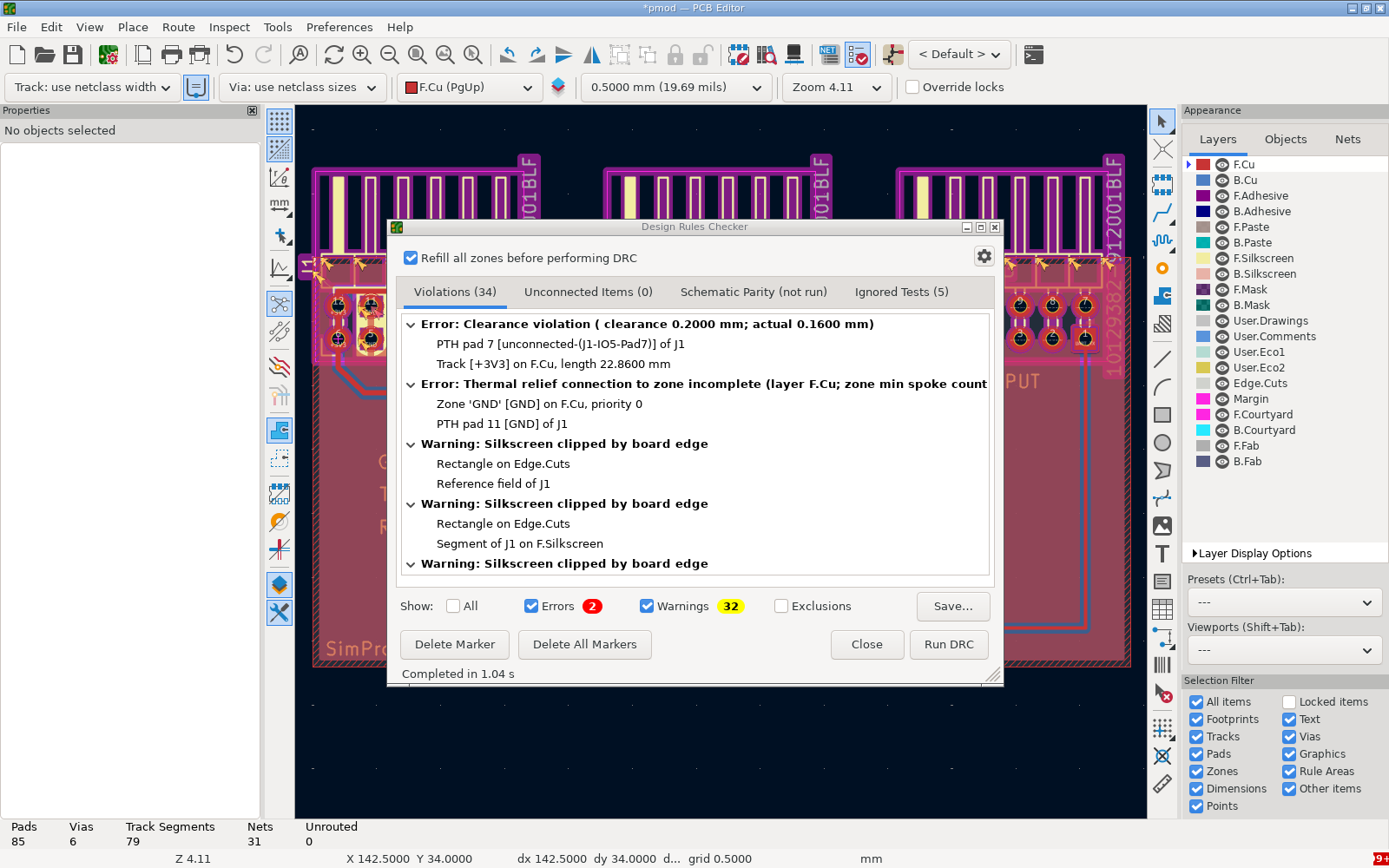
The Design Rules Checker with a clearance violation and a thermal relief error The Design Rules Checker in KiCad 10.0.5 on our board with the track dragged down. It lists a clearance violation between the track and J1’s pad 7 (0.1600 mm against 0.2000 mm), and an incomplete thermal relief on pad 11, because the track now blocks part of that pad’s connection to the GND zone. The other 32 items are the warnings that the board had before.
The dialog’s Schematic Parity tab says “(not run)”. Does that mean your CI doesn’t check parity either?
TipAnswerNo. The editor runs the parity test only when its “Test for parity between PCB and schematic” box is ticked, as you did in Lab 03, Part 4.
ci/build.sh checkrunscheck_board.py, which always passes--schematic-paritytokicad-cli pcb drcand fails on any parity item, warnings included.Run the Lab 05 check. You should see the board check fail inside the build, with the errors that your drag made:
  DRC errors (2):
    clearance                Clearance violation ( clearance 0.2000 mm; actual 0.1600 mm)  [PTH pad 7 [unconnected-(J1-IO5-Pad7)] of J1; Track [+3V3] on F.Cu, length 22.8600 mm]
    starved_thermal          Thermal relief connection to zone incomplete (layer F.Cu; zone min spoke count 2; actual 1)  [Zone 'GND' [GND] on F.Cu, priority 0; PTH pad 11 [GND] of J1]
and then eight rows fail. The first is
check(the board check fails: drc.error 2 (want 0); the fab and images stages didn't run).gerbers,drill,bom,positionandimagesfail becausebuild.shstops at the first stage that fails, so the later stages never made their files.ibomandreportfail too (`ci/build.sh kibot` didn't run, because an earlier stage failed, as in your workflow), because the check, like the workflow, runs KiBot only after the build has passed.Commit the broken board with a message that says what you did, and push. On GitHub you should see a red run. The step “ERC, DRC and schematic parity” fails with the same board check output as above, GitHub skips “Fabrication files”, “Review images” and “KiBot outputs”, and the upload step still runs, so the artifact holds
reports/and nothing else. Our local run of the workflow did the same. Its check step exited 1, the next three steps were skipped, and the artifact had three files,drc.json,erc.jsonandsummary.json.Fix the board by moving the track back, or by undoing the drag with Ctrl+Z before you close the editor. Then save, run the check until it passes, commit, and push. You should see a green run on GitHub, with the full artifact again.
Find the hash of the commit with the planted error (
git log --onelinelists it) and run the check with it:~/pcb101/labs/lab-05-fab-outputs-in-ci/check.sh --planted <hash>It copies that commit’s files into a temporary folder, runs
bash ci/build.sh checkthere, and checks that the board check fails. You should see an eleventh row,ok planted f1b503c, an earlier commit on this branch, fails the board check (drc.error 2), with your own hash and counts, and the last linePASS pmod: 11 of 11 Lab 05 checks ok.
Finishing
You’re done when ~/pcb101/labs/lab-05-fab-outputs-in-ci/check.sh --planted <your planted commit>, run in your own repository, ends with PASS pmod: 11 of 11 Lab 05 checks ok, and your repository’s Actions tab shows a red run on that commit and a green run, with its board-outputs artifact, on a later one.
Questions:
A teammate’s pull request moves a part. Which files in the run’s artifact would you look at first, and why not the
.kicad_pcbdiff?TipAnswerLook first at the renders and the copper plots in
review/, and compare them with the ones from the commit before. Moving one part changes its position, the tracks rerouted to reach it and the zone fills around it, and in the board file’s text diff, the lines that record those changes are hard to read as one change. KiCad files in git shows a “minor” commit to Tiny Tapeout’s demo board that changed 5,770 lines.CI builds Gerbers from the same commit on two days, and their checksums differ. Did the board change?
TipAnswerNot necessarily. Every Gerber, the job file and the drill file carry the date and time of the export (Fabrication outputs), so compare them with those lines removed before you conclude anything.
Submit: nothing for this lab. Keep the workflow; the capstone asks for a green run.
Going further (optional)
- Save the list of outputs in the project as a jobset and run it with
kicad-cli jobset run, so that the list lives in a file next to the board instead of inbuild.sh. We haven’t tried a jobset in this course yet.
Next on the Course path: read Reviewing and ordering a board, then do Lab 06: Review a seeded board.