Parts you can solder by hand
This page answers: which parts can you solder to a board yourself with an iron, and how do you choose footprints so that the board you order is one you can put together?
PCB101 doesn’t ask you to solder anything, and it doesn’t require you to order your board either. If your team does order the board you draw in Lab 03, though, someone will have to assemble it, quite possibly you, and the footprints you choose in the lab decide how hard that job is.
Sizes and their codes
Resistors, capacitors and other two-terminal surface-mount parts come in standard sizes named by a four-digit code, which gives the length and width in units of 0.010 inch. Horowitz and Hill’s example is the “0603” package, 0.06 × 0.03 inch, or 1.5 × 0.75 mm (The Art of Electronics, 3rd ed., p. 1104). KiCad’s footprint names add the metric code, which counts in tenths of a millimetre, so in R_0603_1608Metric the same 0603 part is called 1608, for 1.6 × 0.8 mm.
Horowitz and Hill favour 0603, “or the larger 0805 package, for general prototyping of surface-mount circuits”. They say the smaller sizes, 0402 and below, “are a major pain – you basically have to work under a microscope (and don’t sneeze)”. We follow their advice in this course, so on a board you’ll assemble yourself, use 0603 or 0805 for resistors and capacitors.
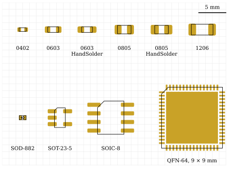
Footprints from KiCad 10.0.5’s own libraries, drawn to one scale on a 1 mm grid by scripts/figures/footprint_sizes.py. The copper pads are gold, and each part’s body is drawn as the footprint’s fabrication layer draws it. The top row is resistors, from left to right 0402, 0603 and its hand-soldering version, 0805 and its hand-soldering version, and 1206. The bottom row is SOD-882, a two-pin diode package; SOT-23-5; SOIC-8; and the 9 × 9 mm QFN-64 that Tiny Tapeout’s SKY130 chip comes in.
KiCad’s hand-soldering footprints
KiCad’s resistor and capacitor libraries have a second footprint for every size, with _HandSolder at the end of its name. Its description reads “IPC-7351 nominal with elongated pad for handsoldering”. It’s for the same part, with longer pads that leave room for the iron’s tip and for a fillet of solder that you can see.
| Footprint | Pad (length × width) | Pad centres from the middle |
|---|---|---|
R_0603_1608Metric |
0.8 × 0.95 mm | ±0.825 mm |
R_0603_1608Metric_Pad0.98x0.95mm_HandSolder |
0.975 × 0.95 mm | ±0.9125 mm |
R_0805_2012Metric |
1.025 × 1.4 mm | ±0.9125 mm |
R_0805_2012Metric_Pad1.20x1.40mm_HandSolder |
1.2 × 1.4 mm | ±1.0 mm |
Each pad ends half its length beyond its centre, so the 0603 hand-soldering pad reaches 1.4 mm from the middle of the part instead of 1.225 mm, and the 0805 one reaches 1.6 mm instead of 1.425 mm. The inner ends of the pads stay where they were, so all of the extra length is on the outside. The capacitor footprints are named the same way (C_0603_1608Metric_Pad1.08x0.95mm_HandSolder, for example), and there are hand-soldering versions of some three- and five-pin packages too, such as SOT-23-5_HandSoldering.
Part sizes on Tiny Tapeout’s boards
Many of the parts on Tiny Tapeout’s boards are smaller than this page recommends. On the SKY130 breakout, every 100 nF capacitor is 0402, while the 1 µF capacitors are 0603 and the 10 µF ones 0805. The DIP dock uses 0402 for 36 of its 37 resistors (the 37th, R15, is a 0 Ω link in an 0805 footprint, and it isn’t fitted) and for its 100 nF capacitors, 0603 for its 1 µF capacitors and its LED, and SOT-353 (SC-70-5) for its two logic gates. Tiny Tapeout can use parts that small because a machine assembles its boards. Its archive of production files has the breakout’s bill of materials, prepared for JLCPCB’s assembly service.
On the breakout, three of the 0 Ω links are 0805: R13, R14 and R15, one on each of the chip’s three supplies. The board’s other fitted 0 Ω links, R2, R4, R5 and R8, are 0603 or 0402. A note on the schematic says that each supply pin “may be monitored or fed through these headers by popping off the relevant resistor (0805s for easier manip)”, so these three links were sized for the person who takes them off by hand. (Measuring current comes back to them.)
Packages with pads you can’t reach
Whether you can solder a part depends as much on whether the iron can reach the joint as on the part’s size.
- SOT-23-5, the package of the breakout’s AP2112K regulator, has its leads out beside the body, on 1.325 × 0.6 mm pads at 0.95 mm pitch. You can see and reach every joint.
- SOIC-8 also has its leads beside the body, on a 1.27 mm pitch.
- SOD-882, the package of 22 of the TVS diodes on the demo board, has a body of 1.0 × 0.6 mm and two pads of 0.4 × 0.7 mm, 0.7 mm apart between centres. Most of each pad is under the body, and only 0.05 mm of it reaches past the end. The whole part is about the size of an 0402, the size at which Horowitz and Hill say you have to work under a microscope.
- QFN-64, 9 × 9 mm with a 0.5 mm pitch, has pads 0.25 mm wide. Each one reaches only 0.375 mm beyond the edge of the body, and the 7.65 × 7.65 mm exposed pad in the middle is entirely underneath the part, where no iron can reach it. The Tiny Tapeout chip comes already mounted on its breakout, so although you’ll draw a footprint for a QFN in Lab 02, you won’t have to solder one.
When you add an ESD array to your Pmod’s dongle header and a buffer to its UART lines in Lab 04, choose parts in packages with their leads beside the body, like SOT-23-5, SOT-23-6 or SOIC-8, and not in a package like SOD-882.
Through-hole parts
The Pmod connectors, like the other through-hole parts on your board, will be the easiest joints to solder. Tiny Tapeout’s Pmod footprint, PinHeader_2x06_P2.54mm_PMODPeriph2B, is for a through-hole angled header, with 1.7 mm pads and 1.0 mm holes on a 2.54 mm pitch. Its joints are large and easy to see, and the pins hold the header in place while you solder them.
Fabricator assembly and safety
If you’d rather not solder, fabricators also assemble boards, as JLCPCB does for Tiny Tapeout’s. Assembly costs more than bare boards, and the fabricator needs your board’s bill of materials and position file, which Fabrication outputs describes. Reviewing and ordering a board covers ordering, and what assembly costs at JLCPCB. The course doesn’t teach soldering or how to do it safely, so if you do solder, do it in a room that’s set up for it and follow that room’s rules.
Check yourself
You need a 100 nF capacitor on a Pmod that you’ll assemble yourself. Which KiCad footprint would you pick?
TipAnswerAn 0603 or 0805 capacitor footprint, preferably the hand-soldering version, such as
C_0603_1608Metric_Pad1.08x0.95mm_HandSolder. Avoid 0402, the size Tiny Tapeout’s boards use for 100 nF, because it’s one of the sizes that Horowitz and Hill call “a major pain” to work with.Why are R13, R14 and R15 on the SKY130 breakout 0805, when its other fitted 0 Ω links are 0603 or 0402?
TipAnswerThey’re the links a person is expected to remove by hand, to measure or feed one of the chip’s supplies, and the schematic says they’re 0805 “for easier manip”. The rest of the board is assembled by machine.
Why can’t you solder a QFN’s exposed pad with an iron, and why does that matter less for the Tiny Tapeout chip than for a QFN on your own board?
TipAnswerThe exposed pad lies entirely under the body of the part, so an iron can’t reach it. The Tiny Tapeout chip comes already mounted on its breakout, so you never solder it. A QFN on your own board would have to be soldered some other way, which this course doesn’t cover, or assembled by a fabricator.
Next on the course path: Lab 03: A Pmod for one project’s pins.