Routing by hand
The capstone asks you to route only three nets, but three are enough to run into every basic idea in interconnect. This page explains those ideas, and you route the nets yourself in the capstone.
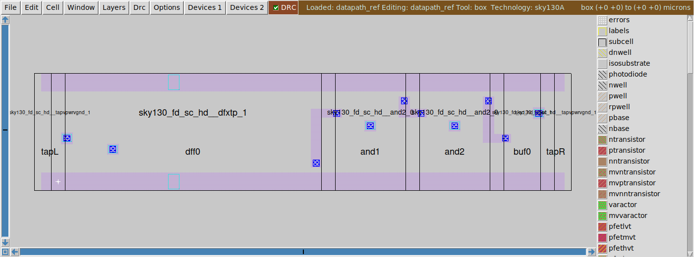
The capstone block with its subcells collapsed, so the cells are outlines and your routing is the only real geometry on screen. Left to right: a tap cell, the flip-flop, two AND gates, the buffer, and another tap. The pink metal1 shapes and the boxed contacts are all of the routing you do by hand.
The layer stack as a routing problem
You can’t connect just any layer to any other. The layers form a single ladder, and a connection can only step from one rung to the next through the contact or via between them:
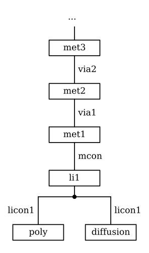
Each of those contacts and vias is a plug of a fixed size, and each plug has enclosure rules for the layers on both sides of it. So a connection from a cell pin to a wire two microns away is built in four steps:
- an
mconon the pin (li1 → metal1), exactly 0.17 µm square - a metal1 pad around it, surrounding the cut by 0.03 µm everywhere and by 0.06 µm on both sides of one axis (
met1.4,met1.5) - metal1 from that pad to the next one
- another pad and another
mconat the far end
The capstone’s pads are 0.29 µm wide around a 0.17 µm cut, which leaves 0.06 µm on each side. That satisfies met1.5 along the x axis, and it’s the smallest width that does.
Which layer to route on
li1 is the layer the cells’ own pins are drawn on, so a wire on li needs no via at either end. The price is resistance: li1 is about 12.8 Ω per square, against 0.125 for metal1, which makes it about a hundred times worse. Use it only for a wire short enough that you can see both ends. Lab 04’s blocks route on li for that reason: the wire there is 2.4 µm long, so saving the vias is worth more than the extra resistance costs.
metal1 is where ordinary local routing goes. Of the cells in the capstone, all but one use metal1 only for their rails, so the band between the rails is free space above every cell except the flip-flop, which has internal metal1 straps of its own.
metal2 and up aren’t used by sky130_fd_sc_hd at all, so if you need to cross the row, go up to them.
The routing band
The rails occupy y = −0.24 to 0.24 and y = 2.48 to 2.96, and two metal1 shapes have to be at least 0.14 µm apart. So any metal1 wire that isn’t part of the supply has to stay between:
y = 0.38 and y = 2.34That leaves 1.96 µm of vertical space, shared by every signal in the row. It’s enough for the capstone, but not for a real block, which is why routers alternate directions.
Why routers alternate directions
The convention is that each metal layer runs in one direction only, and the layers take turns. In SKY130 the standard-cell library’s technology LEF, sky130_fd_sc_hd__nom.tlef, sets metal1 horizontal, metal2 vertical, metal3 horizontal, and so on up to metal5. Metal1 runs the same way as the supply rails in your row.
That can look like bureaucracy, but it’s the only thing that makes routing tractable. Two wires on the same layer going the same way compete for the same track, while two wires on adjacent layers at right angles can cross without interacting. Once every layer has a direction, the question “is there room?” stops being about arbitrary geometry and becomes a question about a grid of tracks, which a computer can answer.
All three of your nets go on metal1, which breaks the rule, but with only three nets you can afford to. While you route them, notice that you can keep the whole picture in your head, and that somewhere around ten nets you no longer could.
Metal already inside a cell
Before you run metal1 across a cell, check what metal1 the cell already has by reading the << metal1 >> section of its .mag file. On the workbench image, and2_0 has 16 metal1 rectangles and buf_1 has 12, all of them in the rails. The flip-flop, dfxtp_1, has 74, including two long horizontal straps across the middle of the cell. Those straps are why the capstone’s D connection can’t put its via at the D label: a pad there would sit 0.07 µm from a strap, which breaks met1.2.
The D pin’s li shape extends down to y = 0.715, clear of the straps, so the via goes down there instead. Finding another place on the same pin to land is the routing move you’ll use most often, and once you’ve done it by hand you’ll know what the tool is doing when it does the same thing.
Pin shapes
A cell’s pin is a rectangle of li, and often it’s several rectangles in different places, all on the same net. buf_1, for example, publishes its output X at three different heights. Any of them is a legal place to land, so pick the one your wire can reach.
You’ll find the coordinates in the cell’s .mag file, on its flabel lines. Here is the one for and2_0’s output X:
flabel locali s 397 425 431 459 0 FreeSans 340 0 0 0 X
port 7 nsew signal output
The units are 0.005 µm, as in every foundry cell’s .mag file (Drawing in Magic shows how your own cells differ), so that pin covers x = 1.985–2.155 and y = 2.125–2.295, measured from the cell’s origin. Add the x position you placed the cell at, and you know where to put the mcon.
The routing loop
The capstone turns this page into a step-by-step procedure: find both pins in absolute coordinates, put an mcon and a pad on each, join them inside the band, and then check your work. You need two checks, because they catch different mistakes. DRC, run under both rule sets (see The full DRC rule set), catches spacing and enclosure errors and missing tap cells, and LVS catches a wire that doesn’t quite land on its pin.