SKY130 layer map
This page lists the layers this course uses, from the bottom of the stack to the top. For each one it gives the name you type in Magic, the number the GDS file uses, and what the layer physically is.
The GDS numbers are written as layer/datatype. They come from the calma lines in $PDK_ROOT/sky130A/libs.tech/magic/sky130A.tech, and they’re the numbers you see in KLayout’s layer panel. The sheet resistances are the resist lines in the same file, converted from milliohms to ohms per square.
| Magic | GDS | Physically | Sheet R |
|---|---|---|---|
nwell |
64/20 | an n-type tub in the p-substrate | 950 Ω/□ |
pwell |
64/44 (marker) | the p-substrate itself. SKY130 has no p-well mask, so Magic draws a p-well only as a marker that lets it reason about the body, and the marker doesn’t become a real layer. | 4400 Ω/□ |
ndiff |
65/20 + 93/44 | n+ silicon at the surface | 120 Ω/□ |
pdiff |
65/20 + 94/20 | p+ silicon at the surface | 197 Ω/□ |
ntap |
65/44 + 93/44 | n+ silicon inside the n-well: a handle on the well | 120 Ω/□ |
ptap |
65/44 + 94/20 | p+ silicon in the substrate: a handle on the substrate | 197 Ω/□ |
poly |
66/20 | polysilicon on the thin gate oxide | 48.2 Ω/□ |
pfethvt |
78/44 | the HVTP implant, which makes a PMOS high-threshold | — |
pc (poly contact) |
66/44 + 95/20 | a tungsten plug from poly to li, plus the NPC blocking mask | — |
ndc / pdc / ntapc / ptapc |
66/44 | the same plug, from silicon to li | — |
li |
67/20 | local interconnect | 12.8 Ω/□ |
mcon |
67/44 | plug from li to metal1 | — |
m1 |
68/20 | metal1 | 0.125 Ω/□ |
via1 |
68/44 | plug from metal1 to metal2 | — |
m2 |
69/20 | metal2 | 0.125 Ω/□ |
via2 / m3 |
69/44 / 70/20 | and upward, to metal5 |
Reading the table
Diffusion and tap are the same GDS layer. diff is 65/20 and tap is 65/44, so they share one mask and differ only in datatype. Whether a piece of either one is n-type or p-type depends on which implant mask (nsdm 93/44 or psdm 94/20) covers it. Physically, a ptap and a pdiff are identical, and they differ only in where they sit: the tap in the substrate, the diffusion in an n-well. That’s why the tap rules and the diffusion rules look so similar.
li is a hundred times more resistive than metal1. Its sheet resistance is 12.8 Ω/□, against 0.125 Ω/□ for metal1. A 10 µm li wire 0.17 µm wide is 59 squares long, so it has about 750 Ω of resistance, while the same wire in metal1 has 7 Ω. That’s why li is called local interconnect: it gets you from a transistor to the wire, and it isn’t meant to be used as the wire itself.
Poly is a poor conductor. Its sheet resistance is 48.2 Ω/□. Poly is the gate, and you can use it as a short wire inside a cell, but it is never used for routing.
The contact ladder
There is exactly one legal route from the silicon up to the metal. The ladder below uses the PDK’s layer names (licon1, li1, met1) rather than Magic’s, with the GDS numbers in parentheses:
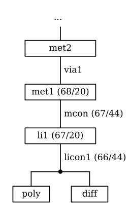
That means you can’t connect poly straight to metal1, or diffusion straight to metal2; you go up one step at a time. Every step is a plug of a fixed size, with enclosure rules at both ends.
Implant masks
nsdm (93/44) and psdm (94/20) decide whether a piece of active silicon is n+ or p+. In Magic you never paint them directly. You paint ndiff or ptap, and Magic generates the right implant when it writes the GDS. You’ll still see them named in DRC messages, though:
NSDM width < 0.40um (diff/tap.5)They also appear in the MASKHINTS_NSDM properties of the foundry’s cells, which is where the library records hand-tuned implant shapes that Magic’s automatic generation would not have produced.
The one implant you do paint is hvtp (78/44), as pfethvt, because nothing else in the layout says which threshold flavour you want for a PMOS.
Viewing layers in KLayout
klayout -nn $PDK_ROOT/sky130A/libs.tech/klayout/tech/sky130A.lyt yourfile.gdsThe layer panel on the right lists every layer in the file with its numbers, and clicking a layer’s eye icon hides it. The fastest way to see the standard-cell rows underneath a routed block is to hide everything above met1.
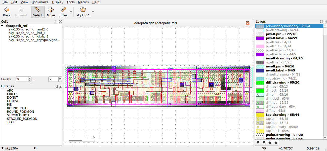
The capstone’s GDS in KLayout. The cell tree on the left has datapath_ref at the top, with and2_0, buf_1, dfxtp_1 and the tap cell under it, and the layer list on the right shows the numbers from the table above.