Stick diagrams
A stick diagram is a layout with all the dimensions thrown away: coloured lines for the layers, crosses for the contacts, and no measurements. What it does record is what order things go in, which is the one thing that’s expensive to get wrong, and you can work that out in ninety seconds on paper instead of an hour in Magic. You’ll sketch one at the start of Lab 03, before you draw anything.
The convention
The convention uses four colours and one symbol, and each has a single rule:
| Green | n-diffusion, drawn horizontally at the level of the NMOS transistors. |
| Yellow / brown | p-diffusion, also drawn horizontally, but higher up, in the n-well. |
| Red | polysilicon, drawn vertically. Every red line that crosses a diffusion makes one transistor. |
| Blue | metal (or li), which can run in any direction, because it sits above everything else. |
| × | a contact, which connects two of the layers listed above it. |
Two more conventions make every cell in a library look alike:
- Power at the top, ground at the bottom, in horizontal metal across the full width of the cell.
- PMOS above, NMOS below. The PMOS transistors sit in the n-well, and the n-well is tied to the positive rail at the top, so this order is more than a matter of taste.
The inverter
   VDD  ═══════════════════════════════
                    ×
        ┌───────────╫───────────┐
   pdiff│           ║           │        (in the n-well)
        └───────────╫───────────┘
                    ║  ×────────────── Y
        ┌───────────╫───────────┐
   ndiff│           ║           │
        └───────────╫───────────┘
                    ×
   GND  ═══════════════════════════════
                    ║
                    A   (poly, vertical)
One red stripe crosses the p-diffusion once and the n-diffusion once, so it makes two transistors, and because it is one stripe, their gates are already connected. That shared gate is why a CMOS inverter is compact: you get the gate connection for free, by drawing one rectangle instead of two rectangles and a wire.
In your AD103 schematic you needed an explicit wire from one gate to the other, so for the inverter the layout is actually simpler than the schematic. That won’t be true of any cell after this one.
The NAND
A 2-input NAND is made of two NMOS transistors in series and two PMOS transistors in parallel.
When two transistors are in series, the drain of one is the source of the other. On a schematic that connection is a wire, but on silicon it means the two terminals are the same piece of diffusion. You draw one strip of diffusion and put two poly stripes across it, and the region between the stripes is the shared node, so it needs no contact, no wire and no extra space.
   VDD  ══════════════════════════════════════
              ×             ×            ×
        ┌─────╫─────────────╫────────────┐
   pdiff│     ║             ║            │      two PMOS, parallel
        └─────╫──────×──────╫────────────┘
              ║      └──────╫─────────────── Y
        ┌─────╫─────────────╫────────────┐
   ndiff│     ║             ║            │      two NMOS, series
        └─────╫─────────────╫──────×─────┘
              ║             ║      └───────────┘
              ×             ║
   GND  ══════════════════════════════════════
              A             B
If you count the contacts on the n-diffusion, there are two, one at each end. The middle of that strip carries current but has no contact, because a contact there would cost area and add junction capacitance to an internal node, and it would gain you nothing in return.
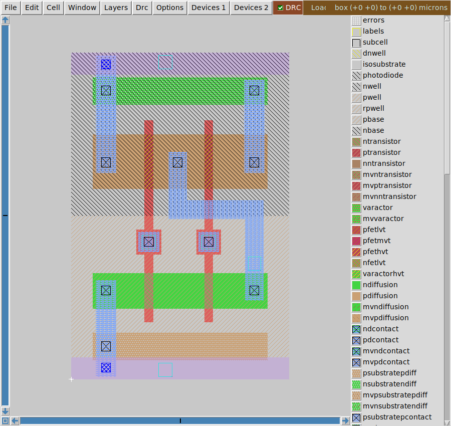
The same sketch drawn in Magic, with its two red poly stripes. The green n-diffusion runs under both of them, with contacts only at the far left and far right and none between the gates. The orange p-diffusion above it has three contacts, because parallel devices alternate source, drain, source.
Choosing the order
For a 2-input gate the order of the transistors barely matters, but for anything bigger it decides whether the cell is one strip of diffusion or three. Each break in the strip costs you a contact, a gap and roughly a quarter of a micron of width.
At this level a rule of thumb is all you need: arrange the inputs so that consecutive transistors in the series chain share a terminal. If you write the gate as a chain of source–drain pairs and you can walk through every transistor without lifting your pen, you can draw it as one unbroken strip. (Formally, you are asking whether the transistor graph has an Euler path.)
You won’t need to choose an order yourself in AD104. In the capstone, though, you’ll place the foundry’s and2_0, which is a single unbroken diffusion strip with three gates on it, and when you do you should recognise that someone chose that order on purpose.