Lab 04: A buffer and an AND gate
In this lab you’ll build two more cells without drawing a single new transistor, because both are made from cells that are already drawn: a buffer is two copies of the Lab 03 inverter, and an AND gate is a NAND gate followed by the same inverter. The work is placing the cells, abutting them, wiring them together and naming their pins, which is also what the rest of a chip is made of.
Package: labs/lab-04-buffer-and-and/
Before you start
- Get Lab 03 to
PASS. - Read Instances and hierarchy. This lab also uses Stick diagrams and Layout versus schematic (LVS).
Time: about 2 hours, not counting the optional Part 7. The full make takes 10 to 15 seconds (10.3 and 13.4 s on two timed clean runs), and nearly all of that is ngspice reading the SKY130 model library for the truth-table simulation. make layout runs only the DRC and LVS part, which takes about 1.5 s, so use it while you are wiring.
Part 1: Look at the NAND
How is the NAND you were given wired, in silicon?
Go into the lab package and build the starting cells:
cd labs/lab-04-buffer-and-and make cells # (re)build mag/my_inv.mag and mag/my_nand2.mag make scaffold # two blocks, each with its two cells already placedmag/my_inv.magis the Lab 03 reference inverter rather than the one you drew, so this lab works on its own. Be careful withmake scaffold: it throws away your work inmy_bufandmy_and2, so run it again only if you want to start over.The NAND comes already drawn, and
tcl/nand2.tclis the script that drew it, commented line by line. Open the cell:make edit CELL=my_nand2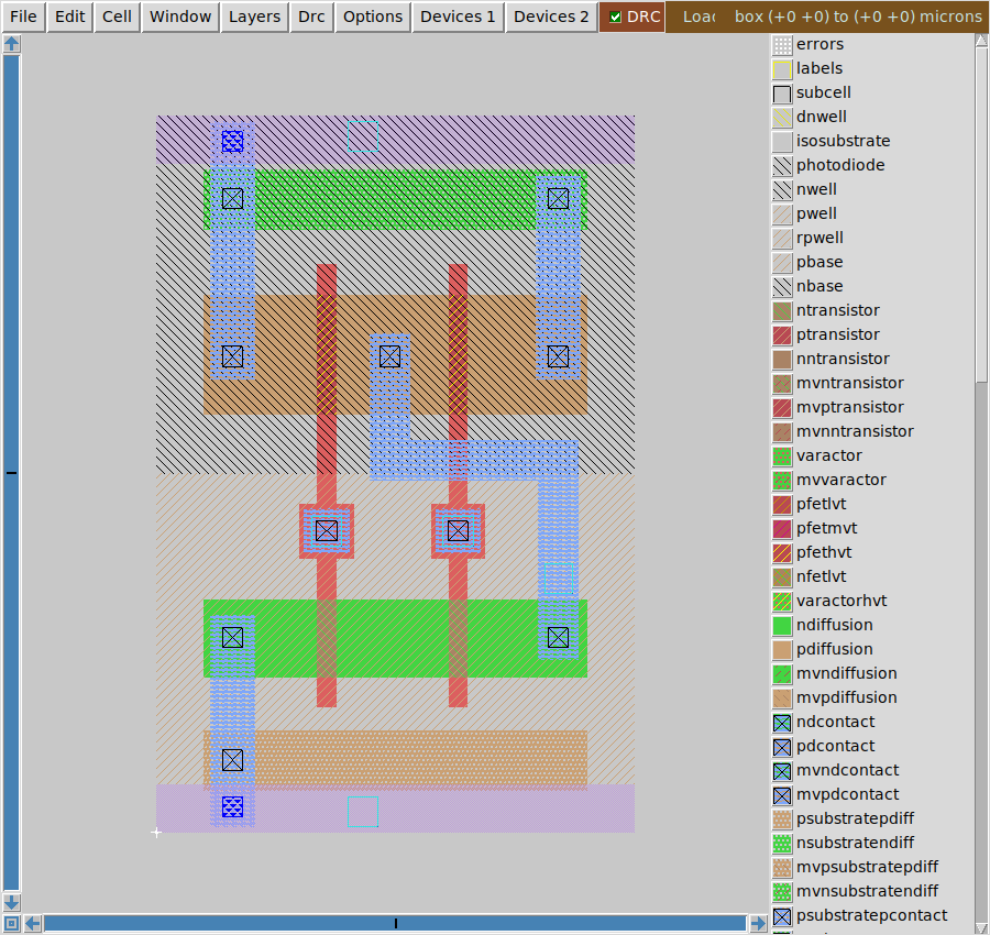
The NAND2 Two red poly stripes cross one strip of green n-diffusion, with contacts only at the far left and far right and nothing between the gates. The two NMOS are in series, and on silicon that means the drain of one and the source of the other are the same piece of doped silicon.
The PMOS above them are in parallel, with three contacts that alternate source, drain, source, and the middle one goes to
Y.Run the layout checks once, so that Magic extracts the blocks:
make layoutIt fails, because nothing is wired or named yet, but it extracts both blocks on the way. Open
results/my_and2.lvs.spiceand find themy_nand2subcircuit, where the two NMOS lines share a node you never named:X0 a_300_260# A VGND VGND sky130_fd_pr__nfet_01v8 ... w=0.65 l=0.15 X3 Y B a_300_260# VGND sky130_fd_pr__nfet_01v8 ... w=0.65 l=0.15a_300_260#is the shared diffusion between the two gates. You never gave it a name, so Magic made one up from its coordinates.
Why is there no contact on the shared node between the two NMOS?
In series, the drain of one transistor is the source of the other, so on silicon they are the same piece of diffusion, and the region between the two gates is itself the shared node. A contact there would cost area and add junction capacitance to an internal node without gaining you anything (Stick diagrams).
You should see the NAND’s single n-diffusion strip under both gates, and a_300_260# in the netlist.
Part 2: Wire the buffer
What do the two inverters already share, and what is missing?
Open the buffer:
make edit CELL=my_bufmake scaffoldgave youmy_bufcontaining twomy_invinstances, at x = 0 and x = 3.0, with the block’s own metal1 rails painted over the row and already labelledVGNDandVPWR. Both cells are 6.00 µm tall with their rails at the same heights, so the rails already abut into two continuous strips and the wells have merged. That means power is already connected, even though you haven’t drawn anything yet.What’s missing is the signal from the first inverter to the second.
inv1’s outputYis an li shape at x = 2.18–2.55, andinv2’s inputAis at x = 3 + 1.24 = 4.24–4.61, both at around y = 2.4, so a single li rectangle can join them:box 2.18um 2.40um 4.61um 2.65um paint li
You should see a single li rectangle running from inv1’s output to inv2’s input, which is all the wiring the buffer needs.
Part 3: Name the buffer’s pins
How do you give the block, rather than the cells inside it, its own pins?
Label the input and output, turn the labels into ports, and save:
box 1.30um 2.40um 1.55um 2.65um ; paint li ; label A c li
box 5.20um 2.42um 5.45um 2.67um ; paint li ; label X c li
select top cell
port makeall
save my_buf
Each of the two label lines paints a small patch of
libefore it places the label. Why not put the label straight on the inverter’s own pin?TipAnswerA label names a net only if it sits on a shape in the cell you’re editing. The input pin you want to name is a shape inside
inv1, so a label placed straight on it would stay inmy_bufwith nothing ofmy_buf’s under it. Magic moves a label like that onto empty space (Moving label "A" from locali to space), where it isn’t attached to any net, andmy_bufwould come out with noAport. Painting your own 0.25 µm patch on top of the pin (it’s the same net, and electrically it adds nothing) gives the top cell a shape of its own to name. The scaffold’s metal1 rails are there for the same reason: they give theVGNDandVPWRlabels top-cell geometry to sit on.Run the layout checks:
make layout
You should see the my_buf row read ok, 0, 0, match. The my_and2 row will keep failing until you wire it in Part 4.
Part 4: Build the AND gate
Can you find the AND gate’s pins yourself?
Open the AND gate:
make edit CELL=my_and2It contains
my_nand2(instancend0) at x = 0 andmy_inv(instancein0) at x = 4.0, with the block’s rails painted and labelled the same way as inmy_buf.nd0’s output is at x = 3.20–3.53, andin0’s input is at 4 + 1.24 = 5.24–5.61, so join them with one li rectangle, as you did in the buffer:box 3.20um 2.40um 5.61um 2.65um paint liPaint li patches and label them:
AandBover the NAND’s two inputs, andXover the inverter’s output. This time you work out the coordinates yourself. You’ll find the NAND’s input li runs on theAandBlines intcl/nand2.tcl. For the inverter’s output, start from theXpatch you painted in Part 3, at x = 5.20–5.45 oninv2’sY. That inverter sat 3.0 µm from the block’s origin andin0sits 4.0 µm from it, so the patch moves 1.0 µm to the right.Run
select top cell,port makeallandsave my_and2, and then runmake layout.
You should see both rows read ok, with 0, 0 and match, and PASS Both blocks are clean under both rule sets.
Part 5: Simulate the AND gate
Does the AND gate really AND, on the extracted layout?
Before you run it, write down the output
Xyou expect for each of the four input rows.Run the full check:
makeThis extracts both blocks, runs LVS on them against
spice/cells_sch.spice, and then simulates the AND gate’s truth table on the extracted layout, with parasitics:TWO BLOCKS, BUILT OUT OF CELLS block DRC default DRC full LVS contains -------------------------------- ------------------------ ---------------------------- ok my_buf 0 0 match my_inv, my_inv ok my_and2 0 0 match my_inv, my_nand2 THE AND GATE, SIMULATED ok A=0 B=0 X = 0.000000 V (expected 0.0) ok A=0 B=1 X = 0.000000 V (expected 0.0) ok A=1 B=0 X = 0.000001 V (expected 0.0) ok A=1 B=1 X = 1.800000 V (expected 1.8) PASS A buffer and an AND gate, both clean under both rule sets, both matching their schematics, and the AND gate really does AND.
The AND gate you just simulated has six transistors, and you didn’t draw any of them in this lab.
src/mktb.py generates the testbench around your netlist’s own port order, instead of assuming one. It does this because Magic numbers a cell’s ports in the order you created the labels, so if you labelled X before A, your .subckt line lists the ports in a different order from the reference’s. A testbench that connected the terminals in the wrong order would give a wrong answer without raising any error.
You should see all four truth-table rows marked ok, and PASS.
Part 6: Meet the pin-swap message
What does netgen say when the circuit is right but two names are on the wrong shapes?
LVS your NAND against a netlist with
AandBexchanged:make swappedNetlists match uniquely. Subcircuit pins: Circuit 1: my_nand2 |Circuit 2: my_nand2 ----------------------------|---------------------------- VPWR |VPWR Y |Y VGND |VGND B |A **Mismatch** A |B **Mismatch** Final result: Top level cell failed pin matching.Read the report as two separate statements, which don’t contradict each other:
- the topology is right: all four devices are wired exactly as the schematic says
- two names are on the wrong shapes: netgen had to swap
AandBto make the match work
Why will nothing else in the flow notice this?
A NAND is logically symmetric in its inputs, so with A and B swapped both simulation and DRC still pass. What the swap does get wrong is the timing model, because in a series stack the input nearer the output is faster than the one nearer ground.
To fix it, swap the two labels in the layout rather than the pin names in the schematic.
You should see Netlists match uniquely and failed pin matching in the same report.
Part 7: Take away the block’s rails (optional)
What happens to the block’s supply ports if it has no rails of its own?
Open the buffer with
make edit CELL=my_buf, and erase the block’s two metal1 rail rectangles in the console:box 0um 0um 6um 0.40um ; erase m1 box 0um 5.60um 6um 6um ; erase m1 save my_bufThe
VGNDandVPWRlabels go too, because they sat on those rectangles, while the inverters’ own rails are left untouched.Run
make layout, and themy_bufrow fails:my_buf 0 0 Top level cell failed pin matching my_inv, my_invand the
FAILline names the missing ports:FAIL my_buf has no port called VGND, VPWR. Its ports are: A X.The two inverters’ rails still abut into continuous strips. Why does the block lose its supply ports anyway?
TipAnswerThe labels went with the rectangles, and the only rail metal left is inside
inv1andinv2. A label over that metal would stay inmy_bufbut land on empty space, as in Part 3, so the block has no shape of its own to carryVGNDandVPWR, and it comes out of extraction with no supply ports at all.Put the rails and their labels back with the scaffold’s own commands (from
tcl/scaffold.tcl), then runmake layoutagain:box 0um 0um 6um 0.40um ; paint m1 box 0um 5.60um 6um 6um ; paint m1 box 2.60um 0.05um 2.85um 0.30um ; label VGND c m1 box 2.60um 5.70um 2.85um 5.95um ; label VPWR c m1 select top cell port makeall save my_buf
You should see my_buf has no port called VGND, VPWR after step 2, and the my_buf row back to ok, 0, 0, match after step 3.
Finishing
You’re done when make ends in PASS on the two blocks you wired and named: both clean under both rule sets, both match in LVS, and all four truth-table rows ok.
Questions:
- Why is there no contact on the shared node between the two NMOS in the NAND? Part 1 answers it.
make swappedreportsNetlists match uniquelyandfailed pin matchingtogether. What is right, and what is wrong? Part 6 answers it.
Submit: nothing for this lab.
Going further (optional)
make ref and make refcheck build and check the reference blocks. The package’s solutions/README.md discusses three decisions in them.
Next on the Course path: read Area, parasitics and delay, then do Lab 05: What it costs.