Lab 03: Draw an inverter
AD103’s capstone was a CMOS inverter that you could simulate. In this lab you draw the same circuit as geometry: two transistors sharing one gate, clean under both DRC rule sets, and checked by netgen to be the circuit you meant.
Package: labs/lab-03-draw-an-inverter/
Before you start
- Finish Lab 02.
- Read Stick diagrams, Extraction and Layout versus schematic (LVS). You’ll use Drawing in Magic constantly.
- Have paper and a pen for Part 1.
Time: about 3 hours. Each make takes about 1.1 s.
The sizes: Wn = 0.65 µm, Wp = 1.00 µm, L = 0.15 µm. These are exactly the numbers in sky130_fd_sc_hd__inv_1, which you read in Lab 01. In Lab 05 you put your cell next to the foundry’s and measure the difference, and because the transistors are identical, the only thing left to compare is the way each cell is drawn. L = 0.15 µm is the SKY130 minimum (poly.1a), but your cell will still be nearly five times the foundry’s area, because area depends on how tightly the shapes are packed rather than on \(L\).
Part 1: Sketch it on paper
What goes where, before any dimensions?
- Draw the inverter stick diagram from Stick diagrams from memory, not copied: PMOS above, NMOS below, one vertical poly stripe crossing both.
- Mark where the two well taps go and which rail each one connects to. The guide page’s sketch leaves them out, and leaving them out is also the most common bug in a first layout, so drawing them by hand once is cheap insurance.
- Decide which side of the cell the input is on and which side the output is on, and why. Part 6 shows where this lab’s reference cell puts them.
The whole sketch takes about ninety seconds.
You should see a sketch with both taps marked, the output on one side and the input on the gate.
Part 2: Start from the frame
What does the frame already give you, and what is missing?
Go into the lab package and lay down the frame:
cd labs/lab-03-draw-an-inverter
make scaffold
make scaffoldthrows away whatever is inmag/my_inv.magand starts again from the frame, so use it now, and after this only when you want to start over.Open the cell in Magic:
make edit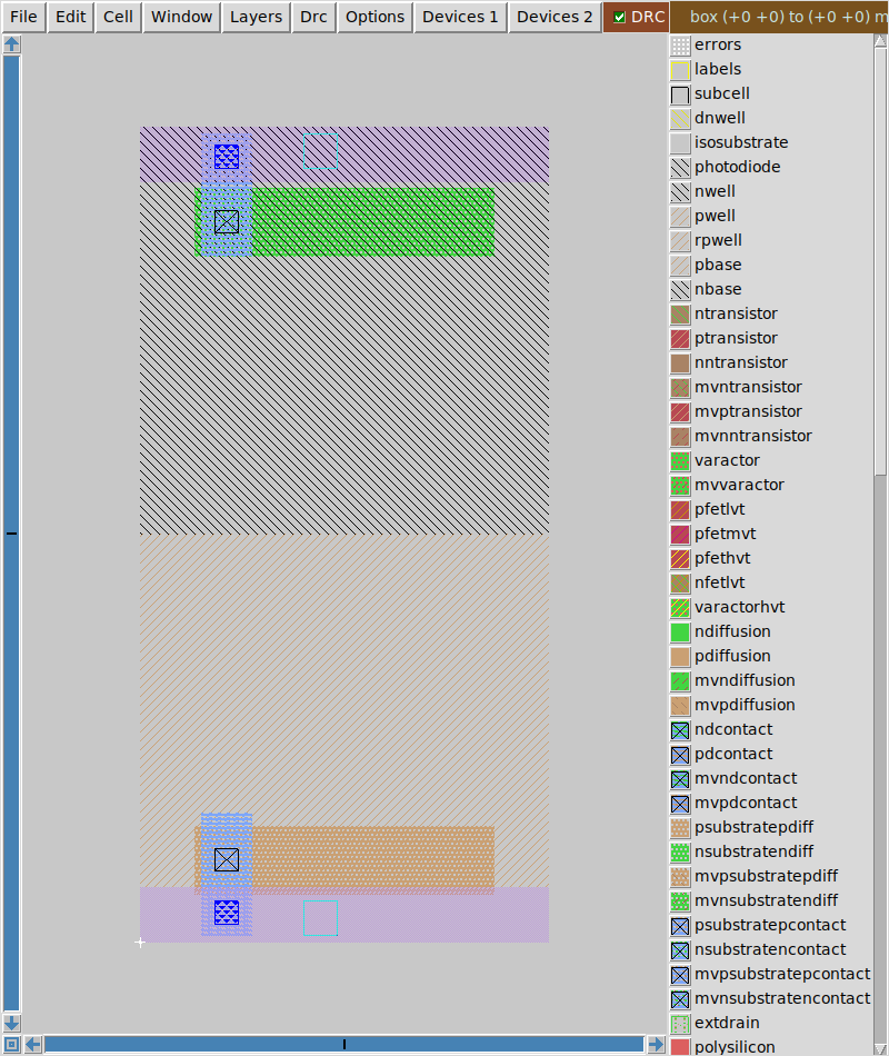
The frame you start from The frame has everything except the transistors. The n-well is the grey hatch across the top half, and the p-substrate is the orange hatch below it. The green strip is the n-well tap and the brown one is the substrate tap, each with a contact and a short li run up to a purple metal1 rail. The middle of the cell is left for you to draw.
The frame already contains:
- the n-well (y = 3.00 to 6.00) and the p-well below it
- the two metal1 supply rails, with
VGNDandVPWRalready labelled - both well taps, contacted, with li up to the rails through
mcon
Compare that with your sketch. The taps you marked are already drawn, so the frame takes care of the tap problem from Lab 02, and what’s missing is the middle of the cell.
Run the checker:
makeWHAT MAGIC FOUND IN my_inv.mag transistors 0 (0 n, 0 p) ports VGND VPWR DRC, default rule set 0 DRC, full rule set 0 LVS Top level cell failed pin matching. FAIL No transistors at all. A transistor is the place where a poly stripe crosses a diffusion. If Magic sees no crossing, either the poly does not overlap the diffusion, or one of them is not the layer you think it is - check the layer name in the title bar as you paint. ...The checker reports every failure in this lab like that, in words, naming the layer or the rule involved. Fix one thing at a time, and run
makeagain after each fix.
You should see FAIL with “No transistors at all”.
Part 3: Draw the two diffusions
How big is each diffusion, and is a diffusion on its own a transistor?
In the
tkconconsole (or by painting with the mouse):box 0.40um 1.30um 2.60um 1.95um paint ndiff ;# 0.65 um tall. The height IS W. box 0.40um 3.50um 2.60um 4.50um paint pdiff ;# 1.00 um tall, inside the nwellThe n-well starts at y = 3.00, so the PMOS diffusion clears its edge by 0.50 µm, which is comfortably more than the 0.18 µm that
diff/tap.8needs.Save:
save my_invmakereadsmag/my_inv.magfrom disk. Painting in Magic changes only what’s on your screen, and the file stays as it was until yousave. Until then, everymakereports on the last version you saved, and neither Magic normakewarns you that this is why the output hasn’t changed. From here on, save before everymake.Before you run
make, predict how many transistors it will find.TipAnswerNone. A transistor is the place where a poly stripe crosses a diffusion, and there’s no poly yet, so a diffusion on its own isn’t a transistor.
Run
makein the terminal.
You should see still transistors 0.
Part 4: Draw the gate
Where does the stripe go, and what sets W and L?
Paint the poly stripe:
box 1.35um 1.05um 1.50um 4.75um
paint poly
The stripe is 0.15 µm wide, and that width is the transistors’ L. It runs from below the NMOS diffusion to above the PMOS one, overhanging each by 0.25 µm, because a gate that stops inside the diffusion leaves a leakage path round its end (
poly.8).save my_inv, then runmake.
You should see two transistors with the right W and L, and DRC still at zero under both rule sets:
      transistors            2   (1 n, 1 p)
        X0   sky130_fd_pr__nfet_01v8          W=0.65  L=0.15
        X1   sky130_fd_pr__pfet_01v8          W=1  L=0.15
The checker also complains that X1 is a pfet_01v8 where it expected a pfet_01v8_hvt. Leave that for now; you’ll fix it in Part 8.
Part 5: Add the contacts
What do the contacts need around them?
Paint four contacts, each exactly 0.17 × 0.17 µm:
box 0.55um 1.55um 0.72um 1.72um ; paint ndc     ;# NMOS source
box 2.28um 1.55um 2.45um 1.72um ; paint ndc     ;# NMOS drain
box 0.55um 3.90um 0.72um 4.07um ; paint pdc     ;# PMOS source
box 2.28um 3.90um 2.45um 4.07um ; paint pdc     ;# PMOS drain
The gate needs a contact too, but it can’t sit on the 0.15 µm stripe.
licon.8asks for 0.05 µm of poly all round a 0.17 µm cut, and that takes a stripe 0.27 µm wide. Instead, draw a landing pad of poly in the gap between the diffusions and put the contact on that:box 1.20um 2.30um 1.65um 2.75um ; paint poly box 1.34um 2.44um 1.51um 2.61um ; paint pcsave my_inv. Before you runmake, predict whether the DRC count goes up or stays at zero.Run
make.
You should see DRC jump to 35 under both rule sets, with three entries under rules broken:
      rules broken:
        Local interconnect overlap of poly contact < 0.08um in one direction (li.5)
        Local interconnect overlap of diffusion contact < 0.08um in one direction (li.5)
        Local interconnect minimum area < 0.0561um^2 (li.6)
Why did five correctly sized contacts break two li rules?
Each contact came with its own patch of li exactly the size of the cut, but li has to overhang a contact (li.5). That 0.17 µm square of li is also smaller than li’s minimum area of 0.0561 µm² (li.6).
In Part 6 you fix all 35 at once.
Part 6: Wire it in li
Which contacts join which, and how wide does the li have to be?
Paint four li runs. Each one has to overhang its contacts by 0.08 µm on both sides along one axis (
li.5), and the 0.37 µm width is there to leave room for that:box 0.45um 0.05um 0.82um 1.82um ; paint li ;# VGND: tap -> NMOS source box 2.18um 1.45um 2.55um 4.17um ; paint li ;# Y: NMOS drain -> PMOS drain box 0.45um 3.80um 0.82um 5.95um ; paint li ;# VPWR: PMOS source -> tap box 1.24um 2.34um 1.61um 2.71um ; paint li ;# A: the gatesave my_inv, then runmake.
You should see DRC back to 0 under both rule sets, and LVS reporting Top level cell failed pin matching, because the circuit is there but A and Y don’t have names yet.
Part 7: Name the pins
How does netgen know which shape is A and which is Y?
Label the input and output, turn the labels into ports, and save:
box 1.30um 2.40um 1.55um 2.65um ; label A c li
box 2.25um 2.60um 2.50um 2.85um ; label Y c li
select top cell
port makeall
save my_inv
Run
make.
You should see four ports, VGND VPWR A Y, and two transistors. LVS still says Netlists do not match; Part 8 explains why.
Part 8: Fix the PMOS flavour
Why does LVS still fail when DRC is clean and every pin has a name?
Read the device lines in the
makeoutput again:X1 sky130_fd_pr__pfet_01v8 W=1 L=0.15The device is a
pfet_01v8rather than apfet_01v8_hvt, which means you have built the wrong transistor. The foundry’s PMOS is the high-threshold flavour, and the flavour you get is decided by an implant mask that nothing you’ve drawn so far mentions. Why did DRC never complain?TipAnswerBoth are legal devices, so DRC has nothing to object to. Only LVS catches the mistake, because it compares your devices with the schematic’s, and that is the case for always running LVS.
Paint the implant over the PMOS gate region and save:
box 1.35um 3.50um 1.50um 4.50um
paint pfethvt
save my_inv
Run
make.
You should see PASS:
  WHAT MAGIC FOUND IN my_inv.mag

      transistors            2   (1 n, 1 p)
        X0   sky130_fd_pr__nfet_01v8          W=0.65  L=0.15
        X1   sky130_fd_pr__pfet_01v8_hvt      W=1  L=0.15

      ports                  VGND VPWR A Y

      DRC, default rule set  0
      DRC, full rule set     0

      LVS                    Circuits match uniquely.

PASS  Two transistors, the right flavours, the right W and L, four ports,
      zero DRC violations under both rule sets, and netgen agrees your
      geometry is the schematic.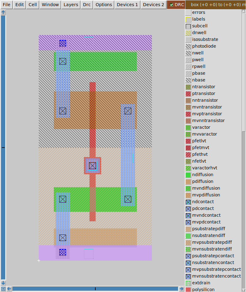
Part 9: Read what you drew
Where in your geometry do w=0.65 and w=1 come from?
Print the netlist Magic extracted from your geometry:
make netlist.subckt my_inv VGND VPWR A Y X0 Y A VGND VGND sky130_fd_pr__nfet_01v8 ad=0.715 pd=3.5 as=0.6175 ps=3.2 w=0.65 l=0.15 X1 Y A VPWR VPWR sky130_fd_pr__pfet_01v8_hvt ad=1.1 pd=4.2 as=0.95 ps=3.9 w=1 l=0.15 .endsExtraction explains every field. Your port order depends on the order in which you created the labels, so it may differ from the reference’s.
Open
mag/my_inv.magin a text editor and find the<< ndiff >>section. The file has nomagscaleline, so one unit is 0.01 µm, and the section’srectlines together span40 130to260 195. That’s your n-diffusion, 0.40 → 2.60 µm by 1.30 → 1.95 µm, which Magic has split into tiles. Drawing in Magic explains the units.
You should see w=0.65 and w=1, both at l=0.15, and you should be able to point at the rectangle whose height is w=0.65.
Finishing
You’re done when make ends in PASS on your own mag/my_inv.mag, and make netlist shows two devices, w=0.65 and w=1, both at l=0.15.
Questions:
- Which rectangle’s height is
w=0.65? Part 9, step 2 answers it. - Why did your cell need LVS, as well as DRC, to show that it was the wrong circuit? Part 8 answers it.
Submit: nothing for this lab.
Going further (optional)
After yours passes, compare it with the reference:
make refcheckruns every check on the reference cell instead of yours.tcl/inverter.tcldraws the reference cell command by command, with a comment on every line saying which rule the number comes from. It didn’t come out right the first time either: the package’ssolutions/README.mdshows the 62 violations its first version had.
Next on the Course path: read Instances and hierarchy, then do Lab 04: A buffer and an AND gate.