Capstone: Place and route
You’ll place four standard cells in a row, route three wires between them by hand, and then measure how fast you can clock what you built. This is the job a place-and-route tool does, at a scale you can hold in your head, so that when you watch a tool do it for a hundred thousand cells you know what you are looking at.
Package: labs/capstone-place-and-route/
Before you start
- Finish Labs 01–05.
- Read Routing by hand and What sets the clock frequency. Instances and hierarchy covers placing cells, and why a label on a subcell’s shape does not name your block.
- Keep the DRC error decoder open in another tab.
Time: about 3 hours, and about half of that goes on routing. make layout runs only DRC and LVS and takes about 1.4 s, so it’s the one to use while you route. The full make adds the timing simulation and takes about 15 seconds (12.6 to 15.6 s on four timed clean runs).
The circuit:
   Q  = DFF(CLK, D)          sky130_fd_sc_hd__dfxtp_1
   n1 = Q  AND A             sky130_fd_sc_hd__and2_0
   n2 = n1 AND B             sky130_fd_sc_hd__and2_0
   Y  = BUF(n2)              sky130_fd_sc_hd__buf_1
That’s a flip-flop, two AND gates and a buffer. Together they make a register bit with some logic after it, which is the most common four-cell cluster in any synchronous chip. Because it has a clock, the timing question at the end of the lab is a real one.
Part 1: Look at the placement
What does a row of four standard cells look like before you wire anything?
Go into the lab package, lay down the placement, and open it:
cd labs/capstone-place-and-route
make scaffold     # four cells placed, nothing wired
make edit
Be careful with
make scaffold, because it throws away your routing. Use it now, and after that only when you want to start over.It places the four cells at x = 0, 7.36, 9.66 and 11.96. Those numbers are a running total of the cells’ widths, which come from each cell’s
FIXED_BBOXproperty. Every cell in the library is 2.72 µm tall with its rails at the same heights, so the rails abut into two continuous strips and the wells merge. At this scale placement is just arithmetic, andtcl/place.tclis nothing more than fourgetcellcalls.Before you run the layout checks on the bare placement, predict the DRC count under each rule set. The foundry’s inverter in Lab 01 is a clue. Then run them:
make layoutYOUR BLOCK outline 13.72 x 3.20 um = 43.90 um2 cells placed 2 x and2_0, 1 x buf_1, 1 x dfxtp_1 cells in the row and2_0, buf_1, dfxtp_1 ports (none) DRC, default rule set 0 DRC, full rule set 32 LVS Top level cell failed pin matching rules broken: All nwells must contain metal-connected N+ taps (nwell.4) P-diff distance to N-tap must be < 15.0um (LU.3) N-diff distance to P-tap must be < 15.0um (LU.2)The same geometry gives zero violations under one rule set and thirty-two under the other, before you have drawn a single wire. You’ll fix the thirty-two in Part 5.
You should see DRC, default rule set 0 and DRC, full rule set 32.
Part 2: Check what is above each cell
Where can your metal1 go without hitting metal1 that is already inside a cell?
and2_0 and buf_1 contain metal1 only in their rails, but dfxtp_1 has metal1 inside the cell as well, and your routing has to keep clear of it.
List the flip-flop’s metal1:
awk '/<< metal1 >>/,/<< labels >>/' \
  $PDK_ROOT/sky130A/libs.ref/sky130_fd_sc_hd/mag/sky130_fd_sc_hd__dfxtp_1.mag
If you add
| grep -c '^rect'to the command, it counts the rectangles instead, and you get 74 fordfxtp_1. Run the same count onsky130_fd_sc_hd__and2_0.magandsky130_fd_sc_hd__buf_1.magand you get 16 and 12, all of them in the rails.Find the flip-flop’s two internal metal1 straps, at y = 1.415–1.645 and y = 1.755–1.985, which run most of the cell’s width. The file is in units of 0.005 µm, so look for rectangles between y = 283 and 397.
The obvious place for the
Dinput’s via is at the D label, around y ≈ 1.19. Work out what a metal1 pad there would do next to the straps (met1.2is metal1 spacing, 0.14 µm), and where else on the D pin you could land instead.TipAnswerA pad at the label would sit 0.07 µm from a strap, which breaks
met1.2. The D pin’s li shape runs all the way down to y = 0.715, so you can take the via down there instead. Finding somewhere else on the same pin to land is the routing move you’ll make most often.
You should see the two straps in the listing, and a plan for where D’s via goes.
Part 3: Route the three nets
How do you get from each pin to the next without touching anything else?
| net | from | to |
|---|---|---|
Q |
dff0/Q at x 6.950–7.120, y 0.425–0.595 |
and1/A at x 7.505–7.675, y 1.785–1.955 |
n1 |
and1/X at x 9.345–9.515, y 2.125–2.295 |
and2/A at x 9.805–9.975, y 1.785–1.955 |
n2 |
and2/X at x 11.645–11.815, y 2.125–2.295 |
buf0/A at x 12.105–12.275, y 1.105–1.275 |
Those coordinates come from the flabel lines in each cell’s .mag file, with the x the cell was placed at added on (Routing by hand shows how).
For each net:
Paint an
mconon each pin, exactly 0.17 µm square, inside the li shape. For example, theQnet starts with:box 6.950um 0.425um 7.120um 0.595um ; paint mconPaint a metal1 pad around each
mcon. A pad 0.29 µm wide leaves 0.06 µm of metal1 on each side of themcon, which satisfiesmet1.5on the x axis.Join the two pads with metal1. Everything has to stay between y = 0.38 and y = 2.34, because the rails occupy y ≤ 0.24 and y ≥ 2.48, and metal1 spacing is 0.14 µm.
save datapath, then runmake layout. If DRC reports a violation, use its rule name to find out what’s wrong and fix it.
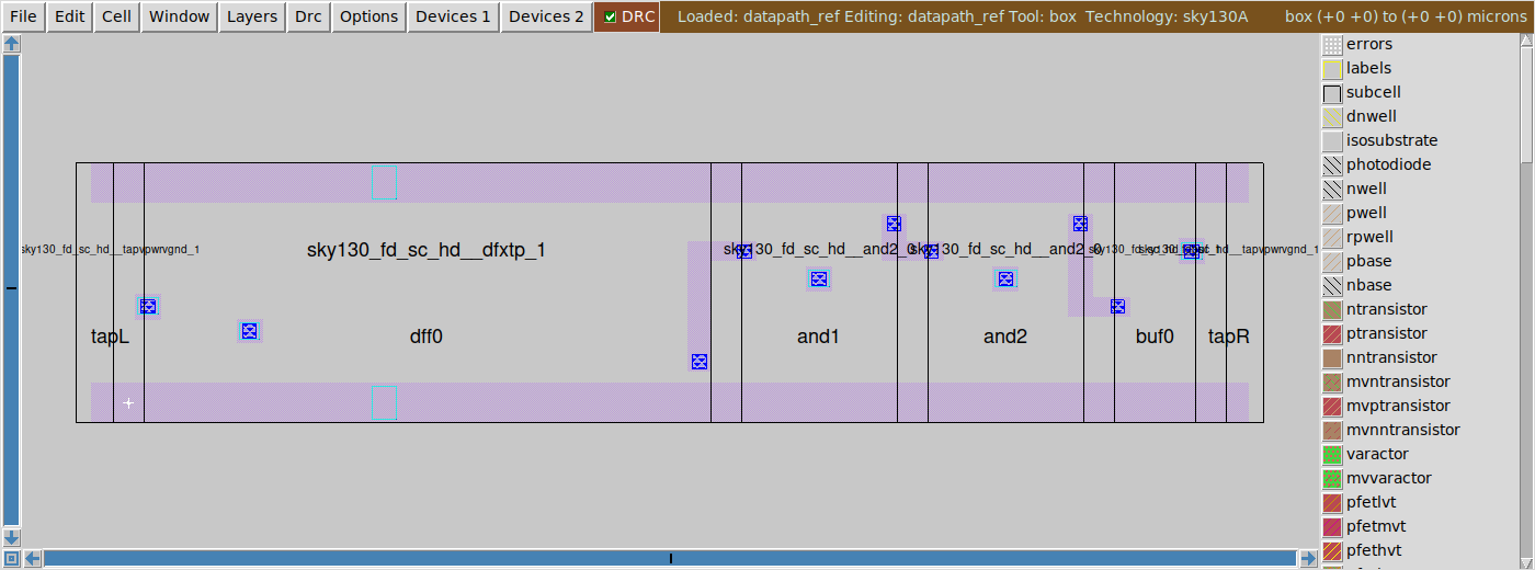
With the subcells collapsed, each cell is drawn as an outline and your routing is the only real geometry on the screen. From left to right: tapL, dff0, and1, and2, buf0, tapR. You add the two taps in Part 5.
You should see DRC, default rule set 0 after all three nets are routed. The full rule set will still report 32, and LVS will still fail, until you’ve done Parts 4 and 5.
Part 4: Bring out the pins
How does your block get pins of its own?
Bring out the block’s own pins,
CLK,D,A,BandY. Each one is anmconon a cell’s li pin, with a metal1 pad over it and a label on the pad. The circuit at the top tells you which cell each pin belongs to:CLKandDgo to the flip-flop,AandBto the free input ofand1andand2, andYcomes from the buffer’s output. Their coordinates are in each cell’sflabellines. Use the spot you chose in Part 2 forD.Paint metal1 rails across the whole row and label them
VGNDandVPWR, so the supply labels sit on geometry that belongs to this cell. If you put the label on one of the standard cells’ own rails instead, it would stay in your block but land on empty space, because the rail under it is the standard cell’s, and a label on space doesn’t name any net.Turn the labels into ports. This is a separate step, and it’s the one everybody skips:
select top cell
port makeall
save datapath
A label is a name written on geometry, while a port is a name that the extractor puts on the
.subcktline.port makeallpromotes every top-cell label to a port. Without it,make layoutreportsports (none)and LVS fails withTop level cell failed pin matching, and the printed advice about putting labels on the top cell’s own geometry won’t help, because yours already are.Run
make layout:ports CLK D A B Y VGND VPWR DRC, default rule set 0 DRC, full rule set 32 LVS Netlists do not match rules broken: All nwells must contain metal-connected N+ taps (nwell.4) P-diff distance to N-tap must be < 15.0um (LU.3) N-diff distance to P-tap must be < 15.0um (LU.2)
You should see ports listing CLK D A B Y VGND VPWR, default DRC at 0, and the full rule set still at 32. LVS has moved on from failed pin matching to Netlists do not match: the block’s pins are all there now, and the taps you add in Part 5 fix the rest.
Part 5: Add the tap cells
What are the 32 violations, and what fixes them?
All 32 violations are about well taps. Nothing in your row ties the n-well to VPWR or the substrate to VGND, because sky130_fd_sc_hd cells are drawn without taps on purpose, as you saw in Lab 01 on the foundry’s own inverter.
The extracted netlist shows the same fault, although it never uses the word “tap”. Look at it:
grep Xbuf0 results/datapath.lvs.spiceXbuf0 buf0/A VGND VSUBS dff0/VPB VPWR Y sky130_fd_sc_hd__buf_1VSUBSanddff0/VPBare invented node names, given to bodies that aren’t connected to anything.You fix this by placing a cell rather than by drawing a shape. Place a
sky130_fd_sc_hd__tapvpwrvgnd_1, 0.46 µm wide, at each end of the row. In the console:box -0.46um 0um -0.46um 0um ; getcell sky130_fd_sc_hd__tapvpwrvgnd_1 ; identify tapL box 13.34um 0um 13.34um 0um ; getcell sky130_fd_sc_hd__tapvpwrvgnd_1 ; identify tapRTwo taps 14.26 µm apart are enough to satisfy
LU.2andLU.3, because those rules only ask for a tap within 15 µm.save datapathand runmake layout. Before you run thegrepfrom step 1 again, predict what the body terminals on theXbuf0line will be now. Then run it; the same line now reads:Xbuf0 buf0/A VGND VGND VPWR VPWR Y sky130_fd_sc_hd__buf_1
You should see 0 under both rule sets and match in LVS.
Part 6: Time it
How fast can you clock what you built?
Run the full check:
makeYOUR BLOCK outline 14.64 x 3.20 um = 46.85 um2 cells placed 2 x and2_0, 1 x buf_1, 1 x dfxtp_1 cells in the row and2_0, buf_1, dfxtp_1, tapvpwrvgnd_1 ports CLK D A B Y VGND VPWR DRC, default rule set 0 DRC, full rule set 0 LVS match HOW FAST CAN YOU CLOCK IT CLK rise -> Y rise 536.17 ps (measured on your extracted layout) D setup at the flop 103.32 ps (sky130_fd_sc_hd__tt_025C_1v80.lib) shortest legal period 639.49 ps f_max 1563.75 MHzMatch the lines to the timing rule:
\[T_{\text{clk}} \ge t_{\text{clk}\rightarrow Q} + t_{\text{logic}} + t_{\text{setup}}\]
The first two terms are simulated on your own geometry, with every parasitic capacitance Magic could find. The third is looked up in
sky130_fd_sc_hd__tt_025C_1v80.lib, because setup time is a property of the flip-flop’s internals and you can’t get it from your layout. As What sets the clock frequency points out, that is the same Liberty file the digital track synthesises against in DD103.Divide your
CLK rise -> Y riseby the foundry cell’sone stagedelay from Lab 05 (32.8 ps on that page), and write down how many inverter delays it is. Why do four gates add up to that many?TipAnswerWith the numbers on these pages, 536 ps is 16 inverter delays. Most of it is the flip-flop’s clock-to-Q, and the
and2_0cells you were given are the weakest AND in the library. Swapping inand2_2would win back some of that time, at the cost of more area.
You should see an f_max printed. The reference block gives 1563.75 MHz.
Part 7: Write the GDS
What do you hand to a foundry, and what is in it?
Write the file a foundry would accept:
make gdsThe reference block’s GDS is 25,778 bytes; yours will be within a few hundred bytes of that. Everything before this step (the
.magfiles, DRC, LVS, the extracted netlist) was for convincing yourself that the layout is right, and GDSII is the file you would actually hand over.Look at it in KLayout:
klayout -nn $PDK_ROOT/sky130A/libs.tech/klayout/tech/sky130A.lyt results/datapath.gds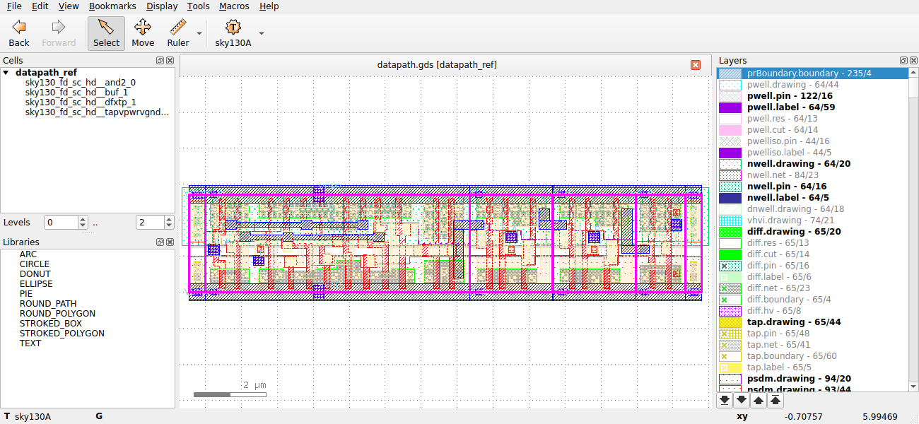
The GDS In the cell tree, notice that the library cells are still separate cells, because the GDS is hierarchical. Magic didn’t regenerate their geometry, either. It copied the bytes from the foundry’s own GDS file, which is what the
GDS_STARTandGDS_ENDproperties in their.magfiles are for.
You should see results/datapath.gds, and the library cells listed separately in KLayout’s cell tree.
Finishing
You’re done when make on your own routed block reports 0 under both rule sets, match in LVS and an f_max, and make gds has written results/datapath.gds.
Questions:
Why did the default rule set report 0 while the full one found 32 violations?
TipAnswerAll 32 break the three well-tap rules (
nwell.4,LU.2,LU.3), and the default rule set leaves those rules out; onlydrc(full)checks them (The full DRC rule set). The cells are drawn without taps on purpose, so the row needed tap cells, which you added in Part 5.Name three reasons a real chip runs at a fraction of your 1.56 GHz.
TipAnswerAny three of: logic depth (a real critical path is twenty to forty levels, not four), wires (delay grows roughly with the square of length, and real nets are hundreds of microns to millimetres long), clock skew and jitter, and margin (sign-off is at the slow-slow corner, 125 °C and low supply, where everything is 30–50 % worse). What sets the clock frequency works through each one.
Submit: nothing for this lab.
Going further (optional)
make ref and make refcheck build and check the reference block. tcl/route_ref.tcl routes it with a comment on every coordinate; the package’s solutions/README.md discusses five of the decisions in it. They’re worth reading once your own block passes.
You have now done by hand, for four cells, what DD103 does with LibreLane for a whole design in about a minute: place cells in rows, insert taps, route, check DRC, check LVS, and write GDS. The tool repeats the same steps a hundred thousand times, guided by a cost function, and it never forgets the taps.
Next on the Course path: this is the last lab in AD104. The home page lists the next courses.