AD104 — Layout
AD103 ended with a CMOS inverter you could simulate: two symbols and a wire. In AD104 you draw that inverter as a layout, the coloured rectangles a foundry turns into masks. You check it the way a real tapeout does, with a design rule check (DRC, can it be manufactured?) and a layout-versus-schematic check (LVS, is it the circuit you meant?). Then you measure what your drawing costs compared with the foundry’s own cell, and you finish by placing and routing a small block of standard cells by hand.
This course is part of the UofT ASIC Team education materials, and it’s published at https://uoftasic.com/ad104/. The labs run inside the shared workspace you set up in IC101.
At a glance
| Who it’s for | Analog-track students who have finished AD103 |
| Track | Analog |
| Prerequisites | IC101 → AD101 → AD102 → AD103, in that order |
| Main tool | Magic 8.3.681, the layout editor. We assume you haven’t used it before, and Getting started starts from there. |
| Also | netgen for LVS, KLayout 0.30.11 for looking at GDS, ngspice 47 for timing what the geometry costs you |
| Math level | Arithmetic and a ruler, because every dimension in this course is a number of microns. |
| Time | About 17 hours, self-paced |
Course path
Work down this table in order. A Read row is one or more guide pages: concepts, figures and worked examples, with nothing to run. A Do row is one lab, where you run every command yourself. Each lab lists the pages to read before you start it.
| # | What | Time | |
|---|---|---|---|
| 1 | Read | Getting started · What a layout is · SiliWiz · Anatomy of a standard cell | 1 h |
| 2 | Do | Lab 01: Open a cell you did not draw. Measure the foundry’s inverter from its layout file, then get DRC, extraction and LVS to agree about it. | 1.25 h |
| 3 | Read | Drawing in Magic · Reading DRC errors · The full DRC rule set | 1 h |
| 4 | Do | Lab 02: Break it on purpose. Fix five inverter layouts, each with one mistake that breaks a real SKY130 rule, until DRC and LVS both pass. | 2 h |
| 5 | Read | Stick diagrams · Extraction · Layout versus schematic (LVS) | 1 h |
| 6 | Do | Lab 03: Draw an inverter. Draw a CMOS inverter in Magic from an empty frame until it is DRC clean and LVS clean. | 3 h |
| 7 | Read | Instances and hierarchy | 30 min |
| 8 | Do | Lab 04: A buffer and an AND gate. Wire an inverter and a NAND into a buffer and an AND gate without drawing a new transistor. | 2 h |
| 9 | Read | Area, parasitics and delay | 30 min |
| 10 | Do | Lab 05: What it costs. Work out what the Lab 03 inverter’s drawing costs in area, then measure what it costs in delay. | 1 h |
| 11 | Read | Routing by hand · What sets the clock frequency | 45 min |
| 12 | Do | Capstone: Place and route. Place four standard cells, route them by hand, and measure how fast the block can be clocked. | 3 h |
The times are estimates, and they leave out the optional parts at the end of some labs. Lab 03 and the capstone take longest, because Lab 03 is the first cell you draw yourself and the capstone is the first block you route.
Keep these open while you work: Magic cheat sheet · DRC error decoder · SKY130 layer map
If you get stuck, ask in the team Discord; nobody expects you to work it out alone at 2 a.m. Getting help says what to include in your question.
The workbench
This course is pinned to the workbench image hpretl/iic-osic-tools:2026.08, which ships Magic 8.3.681, netgen 1.5.323 and KLayout 0.30.11. You start it the way IC101 showed you, and Lab 01 has you load this course’s environment in it and check the Magic, netgen and ngspice versions.
If the environment setup in Lab 01 fails, you can still run make in a lab folder, because every lab pins PDK=sky130A itself and ships its own .magicrc. That means the labs run to completion in a bare container with no setup at all, and each one ends in PASS or FAIL, with a reason.
What this course is about
A schematic says what is connected to what, and a layout says what is where. It’s the layout, rather than the schematic, that decides what a chip costs in area, speed, power and yield.
You will draw a transistor as coloured rectangles, find out from the tools that it cannot be manufactured, fix it, prove it is still the circuit you meant, and then measure what your arrangement of rectangles costs compared with the foundry’s.
The team lead’s summary of layout is that ninety per cent of it is messing things up, and we built the course around that, which is why Lab 02 gives you real broken layouts to fix before you’ve drawn anything of your own.
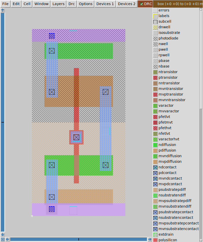
Your inverter at the end of Lab 03: nwell hatched at the top, PMOS in orange p-diffusion, NMOS in green n-diffusion, and one red poly stripe crossing both. That stripe is the gate, and its width is L. The contacts are the boxed X’s, the local interconnect is pale blue, and the two supply rails are purple metal1.
What you’ll do
- Open a cell you did not draw, the foundry’s own inverter, and get four checks to agree about it before you draw anything.
- Fix five broken layouts, each with one mistake that breaks a real SKY130 rule, even though the default rule set calls one of them clean.
- Draw a CMOS inverter from an empty frame until it is DRC clean and LVS clean.
- Turn that inverter into a buffer and an AND gate without drawing a single new transistor.
- Compare your Lab 03 cell against the foundry’s, with parasitics extracted. You’ll find that the same transistors, drawn differently, take 4.8× the area and run 30 % slower in a ring oscillator.
- Place and route four standard cells by hand, get the row clean, and measure the highest clock frequency your layout can run at.
What you’ll have at the end
You’ll finish with a standard cell you drew yourself, a GDSII file of a small block you placed and routed by hand, and a number for how fast that block can be clocked. You’ll also have the habit that makes layout manageable: run the checker, read the rule name, change one thing, and run it again.
Next courses
- AD201 — Analog Signal Processing · AD202 — Mixed Signal
- DD103 — RTL on FPGAs & ASICs, where a tool does the placing and routing you did by hand, for a whole chip, in about a minute