SiliWiz
SiliWiz runs in a browser tab at https://app.siliwiz.com/. You don’t need an account, and there’s nothing to install.
You paint layout layers in SiliWiz, and it shows you the cross-section of the silicon you’ve described and simulates it. It doesn’t model the SKY130 process and it isn’t a production tool, but it’s the quickest way to turn “poly over diffusion makes a transistor” from a sentence you’ve read into something you’ve seen. You can spend twenty minutes with it in Part 8, the optional last part of Lab 01.
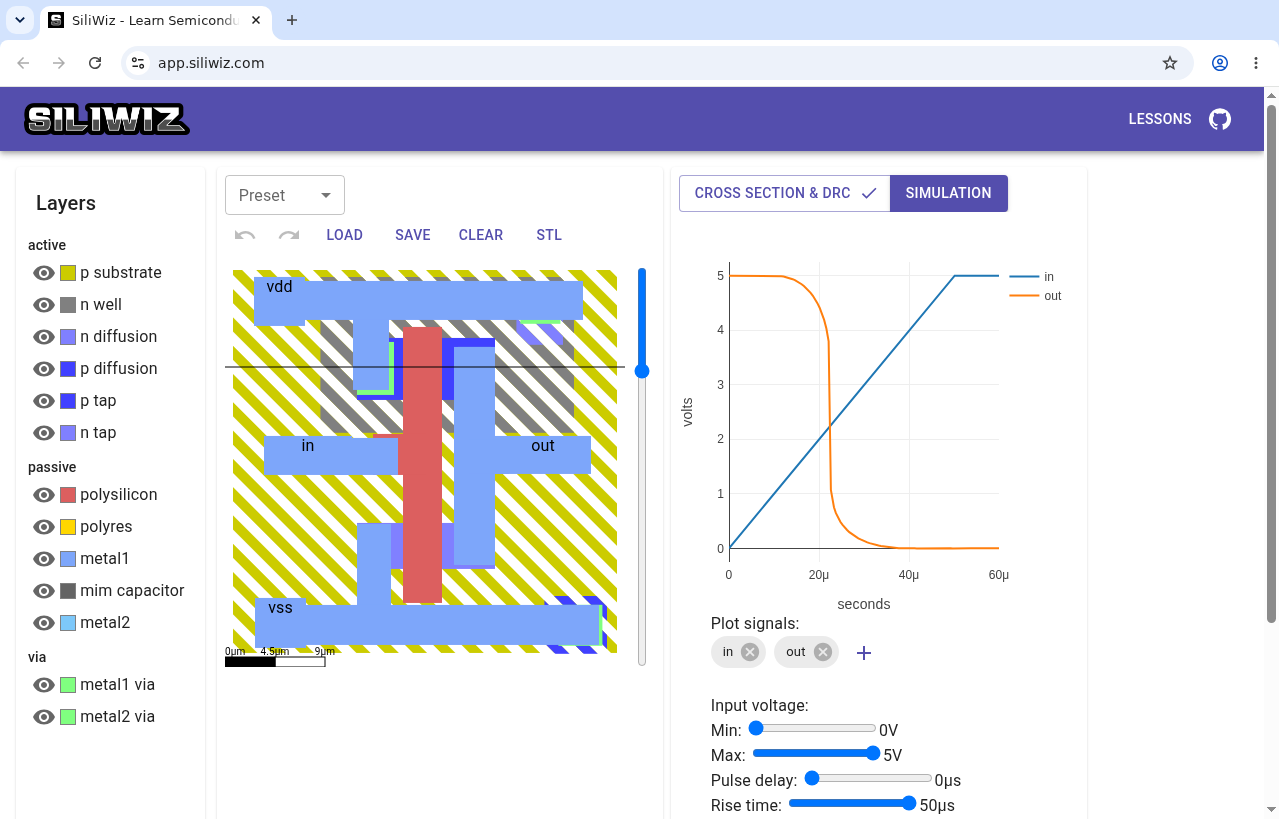
The layer palette runs down the left, the layout you’re painting is in the middle, and the right side shows either the cross-section or, as here, a simulation of what you drew. The black horizontal line across the layout is the cross-section cut, and when you drag the blue slider beside it, the picture on the right changes.
The interface
- LESSONS, at the top right, links to short written walkthroughs at https://tinytapeout.com/siliwiz/: introduction, resistors, capacitors, nmos, pmos, inverter, cmosinverter, divider and parasitics.
- The Preset dropdown above the drawing area loads a finished example.
- The right-hand panel has two tabs: CROSS SECTION & DRC and SIMULATION.
- The vertical blue slider to the right of the layout moves the cross-section cut line. It is the control that matters most, and the rest of the interface is there to support it.
Where SiliWiz differs from a real process
SiliWiz is a teaching model, and it helps to know where it simplifies things:
- The process is invented. The layer names line up with SKY130’s (
n well,p diffusion,polysilicon,metal1,metal2,p tap,n tap), but the dimensions, the design rules and the device models don’t, so don’t carry any number from SiliWiz over into Magic. - It has no LVS. Nothing in SiliWiz checks that what you drew is the circuit you meant, and that turns out to be the harder half of checking a layout; Layout versus schematic (LVS) covers it.
- The cross-section is schematic. It draws each region as a flat-topped block, whereas real doping profiles are gradients.
None of these simplifications gets in the way of what you’ll use SiliWiz for, which is looking at the inside of the wafer. Magic never shows you that view, and SiliWiz is the only tool in this course that does.
Why it is in this course
SiliWiz comes from the TinyTapeout project. The team has put the TinyTapeout shuttle out of scope for these courses (no submissions, no tiles, no deadlines), but that decision was about the shuttle rather than TinyTapeout’s teaching material, and we think this tool is a good one. Nothing in AD104 depends on SiliWiz, so if you skip it, all you lose is the intuition it gives you.