Lab 03: A layout that passes precheck
You’ll replace Lab 01’s two stubs with a real circuit: the CMOS inverter from AD104 Lab 03, placed in your 1x2 tile, with its input on ua[0] and its output on ua[1]. The course gives you the cell and most of its wiring. You move the power stripes and draw the output wire yourself, then check the result three ways: with Magic DRC, with precheck, and with LVS, which precheck doesn’t do. The change goes into main through a pull request in your own repository.
Package: labs/lab-03-a-layout-that-passes-precheck/
Before you start
- Read The analog layout kit, What precheck checks and Your tools and the runner’s tools.
- Finish Lab 02, with both workflows green on
main. - You don’t need to have taken AD104. The cell is DRC and LVS clean as it comes, and you won’t change it.
This lab takes about 1 h 45 min.
Part 1: A branch and a cell
Start the change on a branch of its own, so that it reaches main only through a pull request.
Make the branch and add the lab’s files:
cd /foss/designs/projects/ttsky-ic102-a
git switch -c lab03-inverter
/foss/designs/modules/ic102-a/labs/lab-03-a-layout-that-passes-precheck/start.sh .
You should see:
Added the inverter and its wiring to /foss/designs/projects/ttsky-ic102-a/layout:
 M layout/wires.tcl
?? layout/cells/
?? layout/lvs/
Read the new
layout/wires.tclfrom the top. It places the cell,layout/cells/ic102_inv.mag, at (140, 10) µm; runs each of its supply rails sideways on metal 1 and up a stack of vias to a power stripe on metal 4; and carries the inputAeast on metal 2 toua[0], up to metal 4 and down to the pin. Near the end there’s a TODO where the output wire belongs, and the last line,tieoff 136, ties the 24 digital outputs to ground.Look at
layout/lvs/reference.spice, the circuit the finished tile should contain. Find the one line that says what the inverter connects to, and the 24 lines that tie outputs toVGND.
Check: git status shows the three changes above, and you’re on lab03-inverter.
Part 2: The power stripes
Where do the stripes have to be, and are they legal there?
wires.tclexpects a VGND stripe from x = 136 to 138 µm and a VDPWR stripe from 146 to 148 µm, on either side of the cell. The kit’s script draws its stripes at 1 and 4 µm. Openlayout/init.tcland change its settings block to:set POWER_STRIPES { VDPWR 146um VGND 136um }Before you build, check the stripes against Tiny Tapeout’s rules for analog power pins: “vertical stripes on met4” that “Start within the bottom 10 µm of the module and extend at least to the top 10 µm”, with a “Minimum width of 1.2 um”. Read
draw_power_stripeininit.tcland write down where each stripe starts and ends, how wide it is, and whether it passes. The tile is 225.76 µm tall.TipAnswerdraw_power_stripedraws a box from y = 5 µm to 220.76 µm,POWER_STRIPE_WIDTH(2 µm) wide, starting at the x you give it. 5 µm is within the bottom 10 µm, 220.76 µm is above 225.76 − 10 = 215.76 µm, and 2 µm is more than 1.2 µm, so both stripes pass. Precheck checks the stripes too, in its pin check, against the template.Run
make, thenmake viewto look at the result in Magic on the desktop. You should see the tile, its two new stripes in the right-hand third, and the cell between them, near the bottom edge.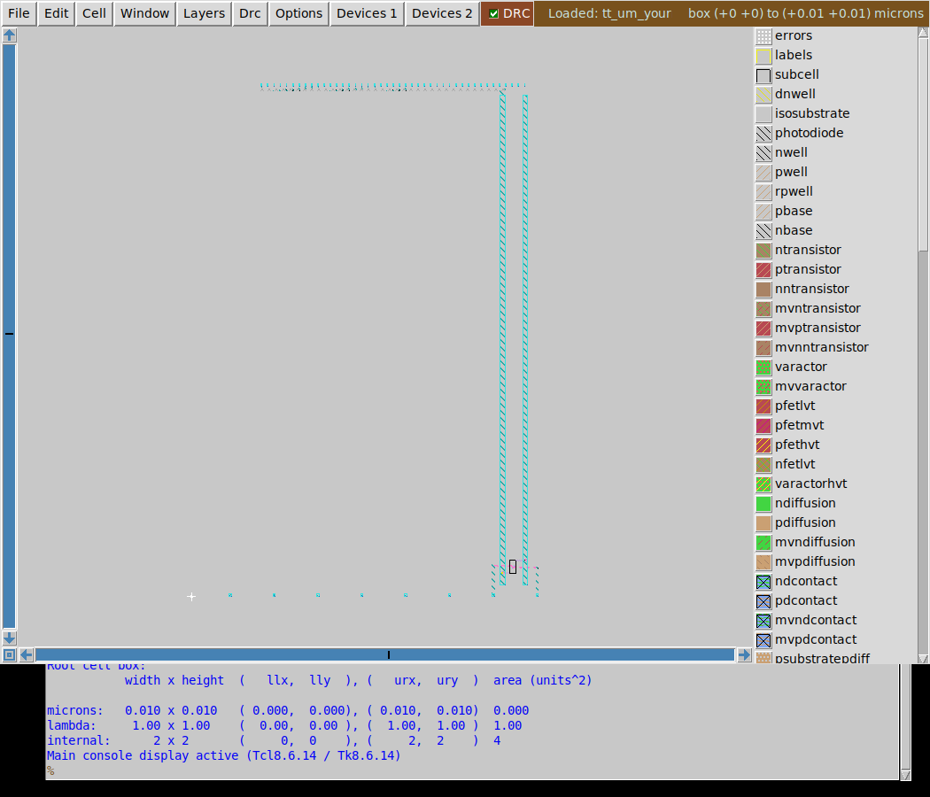
make view: the whole tile in Magic, with the two stripes and the cell between them near the bottom edge.
Check: make ends with wrote gds/tt_um_yourname_ic102.gds and lef/tt_um_yourname_ic102.lef.
Part 3: The output wire
Can you draw a wire that DRC, LVS and precheck all accept?
First see what the checks say about the layout as it is, with the TODO still open. Run
make lvs. You should see:magic: extract a netlist from gds/tt_um_yourname_ic102.gds netgen: the extracted netlist against layout/lvs/reference.spice Final result: Top level cell failed pin matching. (no pin, node is inv0/Y) |ua[1] ua[1] |(no matching pin) full report: layout/build/lvs.reportThe left column is your layout and the right column is the reference. The reference has a pin
ua[1]on the inverter’s output, while in your layout the inverter’s output,inv0/Y, isn’t connected to any pin at all. Precheck sees the same gap in its own way:make precheckfails one check:| Analog pin check | ❌ Fail: Analog pin `ua[1]` is not connected to any adjacent metal but `analog_pins` is set to 2 in `info.yaml`. Either wire up `ua[1]` to your design or decrease `analog_pins` to 1. |Work out the wire on paper before you type anything, using
A’s wire inwires.tclas the pattern. You need four things: a point onY’s locali strip for the contact (the strip runs from x = 142.18 to 142.55 µm and y = 11.45 to 14.17 µm once the cell is placed); a y for the metal 2 that keeps it at least 0.14 µm fromA’s metal 2 at y = 12.3 to 12.75;ua[1]’s x, 132.49 to 133.39 µm; and a metal 4 wire from the via stack down to y = 0. Write the coordinates down.Type the wire into the TODO in
layout/wires.tcl, onepcommand per rectangle, in the same order asA’s: the locali pad,mcon, the metal 1 pad andvia1at the contact; the metal 2 wire; the metal 2 and metal 3 pads,via2andvia3atua[1]; the metal 4 wire. Keep the via rectangles at least as big asA’s, because in Magic a via rectangle includes the metal around its cut.Run
makeandmake drc. You should seeMagic DRC on gds/tt_um_yourname_ic102.gds: 0 errors. If you get errors, the report names the rule, such asMetal2 overlap of Via1 < 0.03um in one direction (met2.5 - met2.4); fix the rectangle it’s about and run both again.Run
make lvs. You should see:Final result: Circuits match uniquely.Run
make precheck. You should seePrecheck passedand all 15 checks ✅.If you’re stuck,
solutions/wires.tclin the lab’s package has one answer. Yours can differ from it in every number and still be right, as long as it passes the three checks.
Check: 0 DRC errors, Circuits match uniquely., and precheck passed, all on the same build.
Part 4: What precheck doesn’t see
Which of the three checks catches a short between the input and the output?
Make a mistake on purpose. In your wire, change the bottom edge of
Y’s long metal 2 rectangle so that it reaches down intoA’s, which runs at y = 12.3 to 12.75. In the reference solution that’s changingp metal2 132.64 13.26 142.6 13.71top metal2 132.64 12.6 142.6 13.71. The two wires are now one piece of metal.Before you run anything, write down which of
make drc,make lvsandmake precheckwill complain.Run
make, then the three checks. In the reference solution with that change, you should seeMagic DRC on gds/tt_um_yourname_ic102.gds: 0 errors, precheck passing all 15 checks, and LVS failing:Final result: Top level cell failed pin matching. (no matching net) |Net: ua[1] (no pin, node is ua[0]) |ua[1] Number of nets: 3 **Mismatch** |Number of nets: 4 **Mismatch**TipWhy do DRC and precheck both pass?The metal itself is legal: it’s wide, well clear of everything else, and joined properly. It’s just connected to the wrong thing, and neither DRC nor any of precheck’s 15 checks compares the layout with what it’s meant to be. LVS does: the extracted circuit has the inverter’s
AandYon one net, calledua[0], where the reference has them on two. So run LVS yourself, every time, before you push a layout.Put the number back, and run
make,make lvsandmake precheckuntil you’re back toCircuits match uniquely.and a pass.Next, try a quicker mistake: comment out the
tieoff 136line, runmake,make lvsandmake precheck, and compare. LVS lists the 24 output pins as unmatched, and precheck passes again. Tiny Tapeout’s analog specs say “Connect any unused uo_out, uio_out and uio_oe pins to GND”, but no automatic check holds you to it. Put the line back and rebuild.
Check: you’re back to a layout that passes all three, and you can say which check caught each mistake.
Part 5: Through a pull request
How does a layout change get into main in a way someone else can check?
Update the pinout to match the new circuit: in
info.yaml, describeua[0]andua[1]as the inverter’s input and output, and updatedocs/info.md. Runmake docs.Commit everything on the branch.
git statusshould showinfo.yaml,docs/info.md,layout/init.tcl,layout/wires.tcl, the two new folders underlayout/, and the GDS and LEF. Then push the branch:git add -A git commit -m "Place the AD104 inverter between ua[0] and ua[1]" git push -u origin lab03-inverterOn GitHub, open a pull request from
lab03-inverterintomain. Your workflows run on every push, so the branch already has adocsand agdsrun, and the pull request shows their results. In the description, say what changed, and paste theFinal resultline ofmake lvsand thePrecheck passedline ofmake precheck. (Paste that line rather than precheck’s last line, which is only the path of its reports.) LVS doesn’t run on GitHub, so the reviewer has no other way to know that you ran it.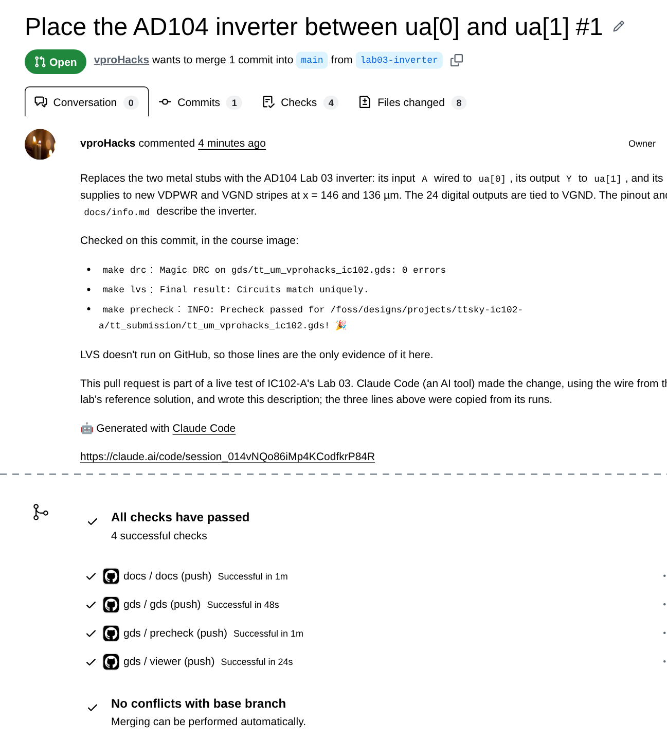
A pull request in your own repository, with the LVS result in its description, and further down, the four checks the branch’s push started: docs, and gds, precheck and viewer. When the branch’s
gdsrun is green in all three jobs, merge the pull request. The merge is a push tomain, so both workflows run again; wait for them.Download the
gds_renderartifact from the merge’sgdsrun and open the PNG. You should see your tile as Tiny Tapeout renders it. The inverter is 3 µm wide in a 161 µm tile, so it’s a speck near the bottom right, with its short wires down toua[0]andua[1]. At this scale the two stripes stand out, and so does the strap along the top edge that ties the 24 outputs to VGND.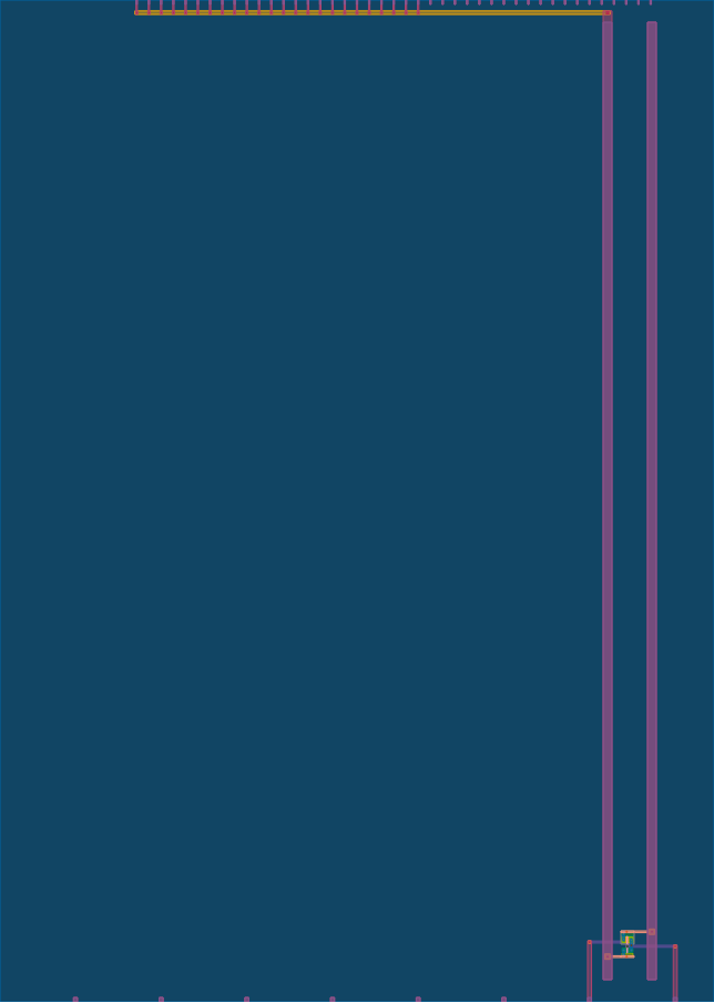
The tile with the inverter from the reference solution, rendered locally with the same gdstk call the gds_render step uses. 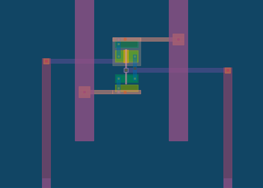
The same render, close up: the cell between its two stripes, the two supply stacks, and the input and output wires running out to ua[0] (right) and ua[1] (left).
Check: the pull request is merged, and the gds run on the merge commit is green.
Finishing
You’re done when the merge commit on your main has a green gds run, with gds, precheck and viewer all passed, and make lvs on that commit prints Final result: Circuits match uniquely.
Questions:
Suppose you’d left the stripes where the kit puts them, VDPWR at 1 µm and VGND at 4 µm, and built the reference solution’s
wires.tclas it is. Which checks would fail?TipAnswerWe tried it: precheck passes all 15 checks, because the stripes are just as legal at 1 and 4 µm, and LVS fails. The cell’s two via stacks now land on empty space at x = 136 and 146 µm, so the inverter’s supplies connect to nothing, and neither do the 24 tied outputs, whose strap ends at the same empty spot.
make lvsstarts its list with(no pin, node is inv0/VPWR) |VDPWRand goes on to the 24 outputs.Your pull request’s diff of
gds/tt_um_yourname_ic102.gdssays only that a binary file changed. What in the pull request lets a reviewer judge the layout?TipAnswerThe text files that built it (
wires.tcl,init.tcl‘s settings, the reference netlist), the runs’ results, precheck’s table, thegds_renderpicture, and the LVS line you pasted. In Lab 04 you review a layout change from those.
Submit: nothing for this lab.
Next on the Course path: read Pull requests and review, Branch rules, Layout files in git and How open-source projects work, then do Lab 04: A change through review.