How a MOSFET works
Everyone says a transistor is a switch, and yet your textbook gives you three different equations for it. The reason is that a MOSFET is a switch you can squeeze, and this page explains what that means.
Think of a garden hose with your hand around it. If you squeeze hard, nothing gets through. If you let go completely, water flows freely, limited only by the tap. In between, which is where every amplifier works, the hose acts as a resistor whose value your hand sets. So one device gives you three behaviours, depending on how hard you squeeze and how hard the tap pushes, and the three textbook equations describe one channel in three different states rather than three different devices.
The four terminals
A MOSFET has four terminals, and only one of them is the hand:
| Terminal | What it does | In the hose picture |
|---|---|---|
| Gate (G) | sets how open the channel is | your hand on the hose |
| Source (S) | where the carriers come from | the tap end |
| Drain (D) | where they go | the open end |
| Body / bulk (B) | the silicon everything is built in | the ground the hose lies on |
The most important thing to know about the gate is what it’s made of. MOS stands for Metal–Oxide–Semiconductor, and the middle word is an insulator. The gate is a plate of conductor sitting on a few nanometres of silicon dioxide (glass) on top of the silicon, so it forms a capacitor with the silicon rather than making an electrical connection to it. ngspice will tell you how big that capacitor is: for the W = 5 µm, L = 1 µm device this course measures, @m.xm1.msky130_fd_pr__nfet_01v8[cgg] comes back as 30.56 fF at \(V_{GS} = V_{DS} = 1.8\) V.
This means that no steady current flows into the gate. Instead of injecting anything into the silicon, you are putting charge on a plate, and the electric field from that charge reaches through the glass and pulls mobile electrons up to the surface of the silicon underneath, out of a p-type body that had few to spare. Those electrons are the channel.
That is why the terminal is called a gate rather than an input: moving it costs charge, but holding it where it is costs nothing. It’s also the reason you’ll read that the gate is high impedance.
The body is a terminal too. In this course the body is wired to the source on every NMOS, which makes the four-terminal device behave like the three-terminal one in your textbook. What moves the threshold is about what happens when the two are at different voltages.
The channel at four bias points
Here is the same transistor at four bias points. Nothing changes from one panel to the next except the two voltages, so watch what happens to the blue layer.
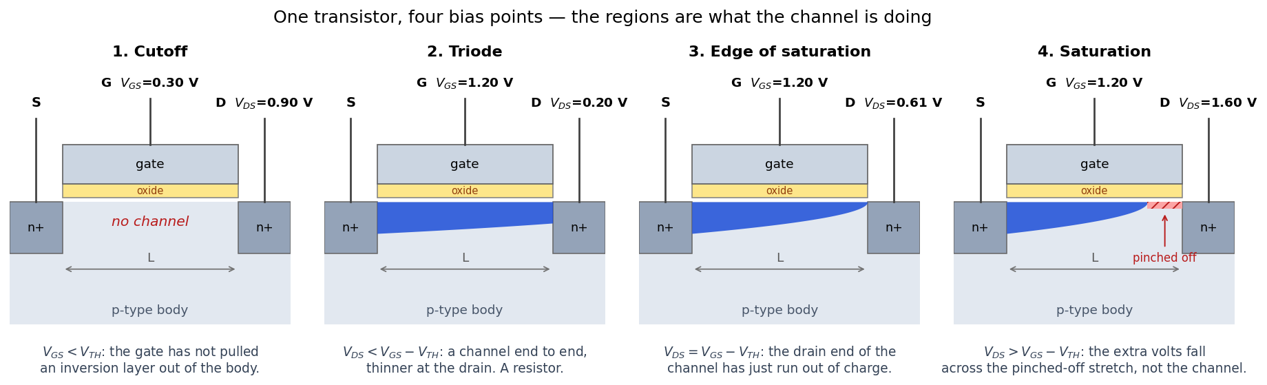
Produced by src/channel_picture.py in the Lab 03 package. The thickness of the blue layer is proportional to the local inversion charge, and the red hatch marks the pinched-off stretch where there is no channel left at all.
Read the panels from left to right:
- Not squeezing hard enough (panel 1). The gate voltage is too low to pull a channel out of the body, so there is no conducting path from source to drain. This is cutoff.
- Squeezing, with a small push (panel 2). A channel runs from end to end. It is a little thinner at the drain, because the drain voltage partly cancels the gate’s pull there, and the current is proportional to the push. This is triode, where the device acts as a resistor.
- The drain end runs out (panel 3). If you push harder, the channel gets thinner at the drain end until, at one particular drain voltage, it has exactly zero charge there.
- Push harder still (panel 4). The zero-charge point moves back from the drain, and all the extra volts you added fall across that pinched-off stretch instead of across the channel. The channel itself sees the same voltage it did in panel 3, so it carries the same current. This is saturation, where the device acts as a current source.
The last panel is the one worth understanding properly. In saturation the current stops increasing because the part of the device that sets the current no longer sees your extra voltage, not because an equation says so.
The squeeze, in numbers
Lab 03 sweeps a W = 5 µm, L = 1 µm nfet_01v8 at five gate voltages, and this is the first table it prints:
== I_D vs V_DS   (W=5, L=1)
   gate voltages read from spice/id_vds.spice: 0.6 0.9 1.2 1.5 1.8
     V_GS  I_D at V_DS=1.8   knee V_DS   channel R at V_DS=10 mV
     0.60         2.005 uA       0.09 V              26648.3 ohm
     0.90        63.876 uA       0.29 V               2529.2 ohm
     1.20       217.505 uA       0.50 V               1288.0 ohm
     1.50       436.080 uA       0.70 V                907.7 ohm
     1.80       696.275 uA       0.89 V                736.9 ohm
Look at the last column first. It is the resistance of the channel, measured with only 10 mV across it, which is small enough that the transistor is unambiguously behaving as a resistor. The resistance goes from 26.6 kΩ to 737 Ω as the gate goes from 0.6 V to 1.8 V, a 36-fold change with no moving parts, controlled by the voltage on a plate that sits on glass, which makes the transistor a dial rather than an on/off switch.
The current at the off end isn’t zero either. With the gate at 0 V and 1.8 V across the device, the same lab measures
== below threshold   (V_DS = 1.8 V)
   V_GS = 0.00 V   I_D = 2.1853e-12 A
That is 2.19 picoamps, 320 million times less than the 696 µA the device passes when it is wide open, but still not zero. Much of The four regions is about that number.
Both numbers matter, for different reasons. The 737 Ω is why a digital gate can charge the next gate’s input in picoseconds, and that sets your clock speed. The 2.19 pA is why a phone’s battery drains while it sits on the table doing nothing. That current is called leakage, and on a chip with ten million transistors it has been the dominant design constraint of the last twenty years.
On-resistance and off-current. If someone hands you a transistor and calls it a switch, ask them what its on-resistance and its off-current are. Both are finite, you can measure both in an afternoon, and the word “switch” tells you neither.
You’ll produce this table yourself in Lab 03, Part 3.
Units on W and L
The units mistake described in Getting started applies to every deck from here on. In SKY130, W and L are plain numbers in microns, with no unit suffix, so W=5 means five micrometres. W=5u asks for a width that falls outside every model bin, and ngspice stops with could not find a valid modelname, a message that mentions neither W nor units. In Lab 03, Part 7 we have you trigger this error once on a MOSFET deck.
What a MOSFET is used for
The regions map onto two jobs:
- Switching. You drive the gate all the way to 1.8 V or all the way to 0 V and never linger in between. That uses cutoff and triode, and the numbers you care about are the 737 Ω and the 2.19 pA. This is how all of digital design uses transistors, including every gate in the DD track.
- Amplifying. You park the gate somewhere in the middle, keep the drain high enough that the channel stays pinched off, and wiggle the gate. That uses saturation, and what you care about is how much the current moves per volt of wiggle. That number is called \(g_m\), and it is the subject of Transconductance and output resistance.
An amplifier and a logic gate are the same device biased in different regions, which is why The CMOS inverter treats a logic gate as an amplifier later in this course.
Check yourself
- Why does no steady current flow into the gate? What does it cost to change the gate voltage?
- In panel 4, the drain voltage is higher than in panel 3. Why is the current the same?
- From the table, roughly what is the channel resistance at \(V_{GS}\) = 1.2 V, and how does it compare with the value at 1.8 V?
- Is a transistor used as a digital switch mainly in saturation, or in cutoff and triode?
Next: The four regions.