Capstone: The CMOS inverter
You’ll draw a CMOS inverter, measure the voltage at which it switches, and size its PMOS two different ways for two different goals. You’ll also run the same circuit as an amplifier, and finish with the current mirror that would bias it.
At the end you’ll have a schematic of a real logic gate, sized by you and verified against a simulation, and it’s the file that AD104 asks you to draw as geometry.
Package: labs/capstone-inverter/
Before you start
Finish Lab 04.
Read The CMOS inverter and The current mirror.
Open a terminal in the workbench, load the environment (you’ll use XSchem in Part 2), and go to the lab folder:
. /foss/designs/common/.designinit
cd /foss/designs/modules/ad103/labs/capstone-inverter
The
MakefilesetsPDK=sky130Aitself, so themaketargets work even without the first line.
Time: about 2.5 hours. make takes about 55 seconds; make mirror and make broken take about ten seconds each. Once make has run, make figures takes a few seconds, and so does make extract, except the first time, when it also runs spice/gain_op.spice and takes about ten.
At the switching threshold the input and output are the same voltage, so both transistors are saturated and carrying the same current:
\[ I_{Dn}(V_{GS}=V_M) \;=\; I_{Dp}(V_{SG}=V_{DD}-V_M) \]
That condition says the currents are equal at \(V_M\), which is not the same as saying the two devices are equally strong at full drive, and the difference between those two statements is what most of this lab is about. The gain at the switching point has the same form as any amplifier’s gain:
\[ A_v = -\,(g_{mn}+g_{mp})\,(r_{on}\parallel r_{op}) \]
Part 1: Run the reference decks
Does your workbench reproduce the reference inverter?
Run the five decks and the checker:
make== spice/vtc.spice wrote results/vtc.txt == spice/vtc_ratio.spice wrote results/vtc_ratio.txt == spice/vtc_long.spice wrote results/vtc_long.txt == spice/drive.spice wrote results/drive.log == spice/delay.spice wrote results/delay.log == checking YOUR NUMBERS ok I_D NMOS W=1 L=0.15 501.0462 uA (reference 501.0462) ok I_D PMOS W=1 L=0.15 200.7478 uA (reference 200.7478) ok NMOS / PMOS drive ratio 2.4959 (reference 2.4959) ok V_M Wn = Wp = 1 0.8380 V (reference 0.8380) ok gain at V_M, L = 0.15 -13.1253 (reference -13.1253) ok V_M Wp = 2.5 0.8827 V (reference 0.8827) ok V_M Wp = 3.5 0.8999 V (reference 0.8999) ok V_M L = 0.5, Wn = Wp 0.7141 V (reference 0.7141) ok gain at V_M, L = 0.5 -116.0341 (reference -116.0341) ok t_pHL Wp = 2.5 30.2508 ps (reference 30.2508) ok t_pLH Wp = 2.5 30.7067 ps (reference 30.7067) ok t_pLH / t_pHL Wp = 1 2.3341 (reference 2.3341) V_out(0.0 V) = 1.800000 V V_out(1.8 V) = 2.129252e-07 V PASS all twelve measured values match the reference runDraw the figures into
results/:make figures
You should see PASS all twelve measured values match the reference run.
Part 2: Draw the inverter
Can you draw an inverter that behaves exactly like the shipped deck?
Open your scaffold:
make edit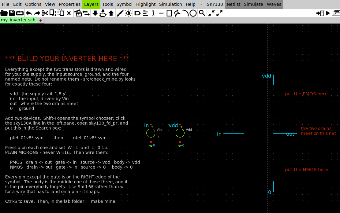
xschem/my_inverter.sch — the supply, the input, the four named nets, and two gaps The scaffold has everything except the two transistors. The nets
vdd,in,outand0are already named and wired. Don’t rename them, becausesrc/check_mine.pylooks for exactly those four names.Add a
pfet_01v8and annfet_01v8(Shift-I, as in Lab 01), both withW=1andL=0.15.Wire the eight pins:
    PMOS   drain -> out    gate -> in    source -> vdd    body -> vdd
    NMOS   drain -> out    gate -> in    source -> 0      body -> 0
The first time through, wire the PMOS body to
0instead ofvdd, on purpose. It’s the pin everyone forgets, so it’s worth seeing what the checker says about it.Save (
Ctrl-S, then Yes) and check your drawing:make mineRead what it says about the PMOS body, then fix the wire, save, and run
make mineagain.make minechecks the things a first inverter usually gets wrong (a missing device, a unit suffix onW, an inventednet7where a wire didn’t land, the PMOS body left on ground) and reports each one in words.When it passes, compare your switching threshold with the reference.
You should see, once the wiring is right:
  YOUR INVERTER
    V_out(0.0 V)              1.800000 V
    V_out(1.8 V)          2.131046e-07 V
    switching threshold       0.838029 V
    gain at V_M               -13.1252
    noise margins H / L     0.8106 / 0.6376 V

PASS  Wn = Wp = 1 um, and your V_M is 0.838029 V against the
      reference 0.838027 V. You drew the same inverter the
      shipped deck describes, and it behaves identically.
Your 0.838029 V and the deck’s 0.838027 V differ by two microvolts, which shows that your drawing and the hand-written deck in spice/vtc.spice are the same circuit. Every schematic you draw is really a claim about a netlist, and comparing it against a deck you already trust is how you check that claim.
Here is the finished version, to compare against once yours works:
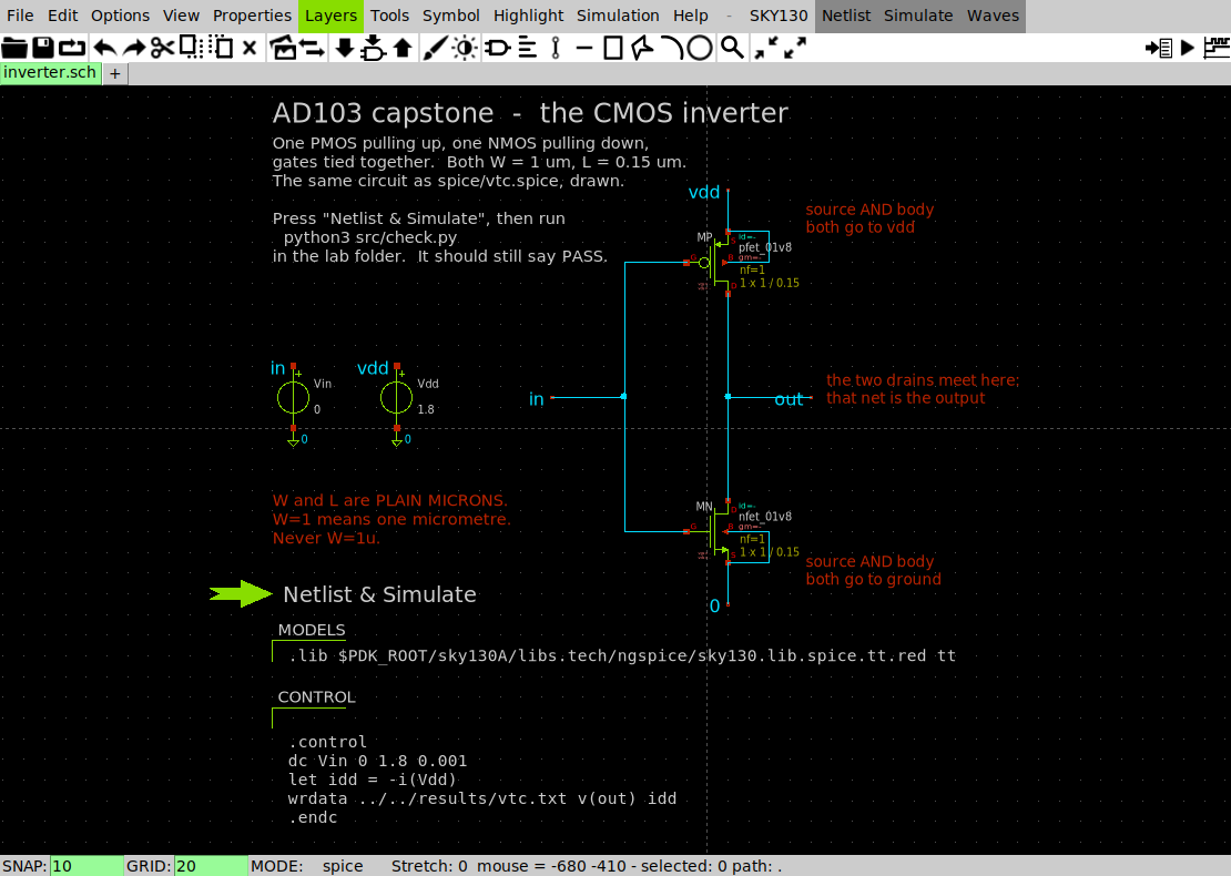
One pfet_01v8 above one nfet_01v8, with the drains tied to out and the gates tied to in. The .lib line and the .control block are carried on the same sheet in two code_shown symbols.
Part 3: The switching threshold
Where does an inverter with \(W_n = W_p\) switch?
Before you look, write down where you think an inverter with \(W_n = W_p\) switches. There’s only one plausible guess, but write it down anyway so that you can compare it with the result.
Print the analysis, and read block 2:
make extractswitching threshold V_M 0.838027 V (V_DD/2 would be 0.900000) steepest slope -13.1253 at V_in = 0.814 V V_IL / V_IH 0.706 / 0.940 V V_OH / V_OL 1.7506 / 0.0684 V noise margin high / low 0.8106 / 0.6376 VOpen
results/ad103-inverter-vtc.png: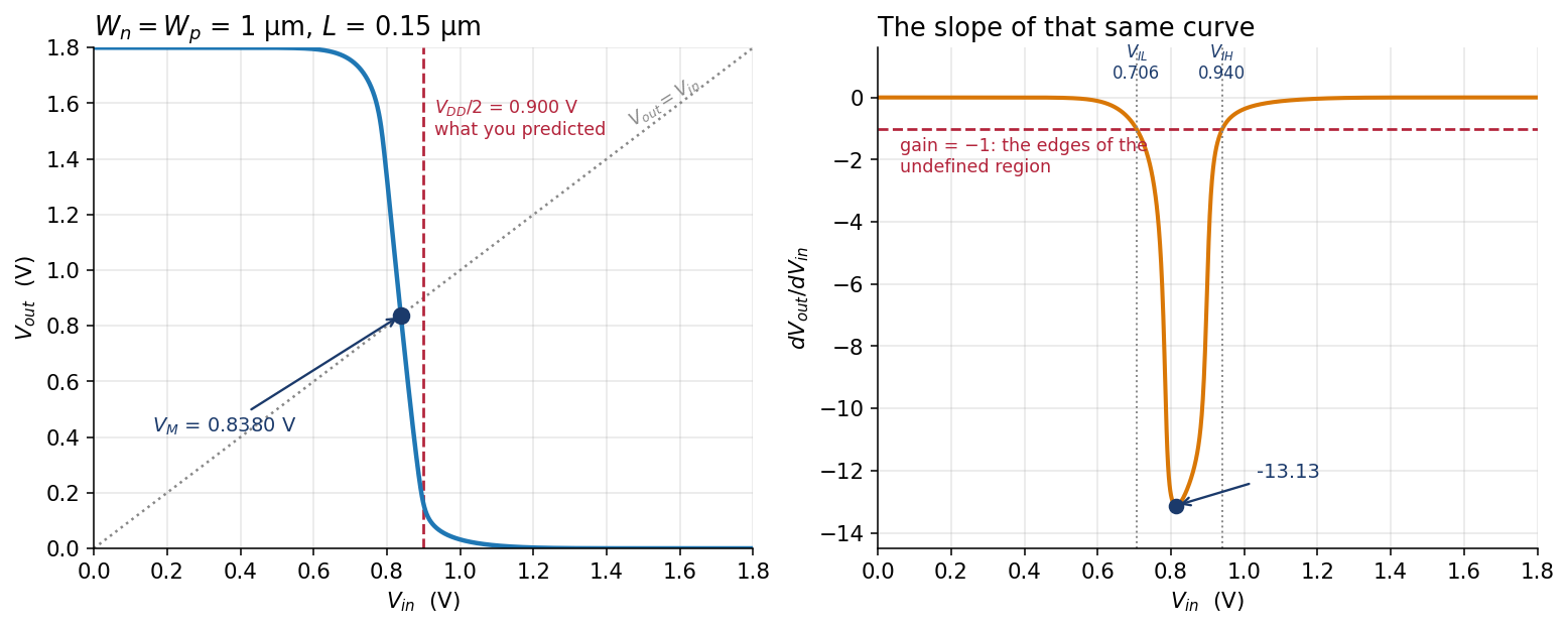
The VTC of the Wn = Wp inverter, and its slope \(V_{IL}\) and \(V_{IH}\) are the two inputs at which the slope passes through −1, marked on the right-hand plot. Between those two inputs the gate amplifies noise instead of rejecting it, and the noise margins are the room left on either side of that region.
You should see \(V_M\) = 0.838027 V, which is 62.0 mV below the 0.900 V of \(V_{DD}/2\).
Why does the \(W_n = W_p\) inverter switch below \(V_{DD}/2\)?
The pull-down is the stronger device (Part 4 measures by how much: 2.4959×), so it takes less input voltage than you might expect for it to drag the output down. \(V_M\) is the input at which the two currents are equal. It isn’t the threshold voltage of either device (769.27 mV for the NMOS, the vth Lab 01’s make bins printed, and 510.03 mV for the PMOS), and it isn’t their average either. That makes it the first parameter in this course that belongs to a circuit rather than to a single transistor.
Part 4: Size the PMOS from the drive ratio
If you widen the PMOS by the drive ratio, does \(V_M\) land at 0.9 V?
Read block 1 of
make extract, the drive of each transistor on its own:NMOS, gate and drain at 1.8 V 501.0462 uA PMOS, gate and drain at 0 V 200.7478 uA NMOS / PMOS 2.4959The 501.0462 µA is the same number Lab 01 gave you, because it’s exactly the same device at exactly the same bias.
The PMOS is the weaker device, so the obvious fix is to widen it to match. Using the drive ratio, predict \(V_M\) for \(W_p\) = 2.5 µm.
Read block 3, five pull-up widths, and open
results/ad103-inverter-ratio.png: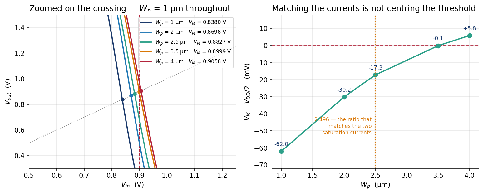
Five pull-up widths, and the error in V_M against W_p Wp (um) Wp/Wn V_M error vs 0.9 V gain 1 1.00 0.838027 V -61.97 mV -13.1253 2 2.00 0.869826 V -30.17 mV -12.8834 2.5 2.50 0.882739 V -17.26 mV -11.8856 3.5 3.50 0.899865 V -0.13 mV -11.2590 4 4.00 0.905807 V +5.81 mV -11.2846
You should see 0.882739 V for \(W_p\) = 2.5 µm, which is 17.3 mV below centre instead of 62.0 mV, so it’s better but still not centred. The width that does centre it is 3.5 µm, giving \(V_M\) = 0.899865 V, 0.13 mV from the middle.
Why didn’t matching the drive ratio centre \(V_M\)?
You matched the currents at full drive, but \(V_M\) is set by where the currents match at the crossing. At \(V_M\) the NMOS has \(V_{GS} = V_M\) and the PMOS has \(V_{SG} = 1.8 - V_M\), so neither device is at 1.8 V, and currents that are equal at full drive aren’t equal there.
Part 5: Time the three inverters
Which pull-up width gives equal rise and fall delays?
Before you read it, guess which of the three inverters (\(W_p\) = 1, 2.5 and 3.5 µm) has the most equal pair of delays.
Read block 4 of
make extract. The delays come fromspice/delay.spice: a real edge, a 10 fF load, and.measfor rise and fall delay.Wp (um) t_pHL t_pLH pull-up / pull-down 1 27.7001 ps 64.6539 ps 2.334 2.5 30.2508 ps 30.7067 ps 1.015 3.5 31.7807 ps 24.1077 ps 0.759
You should see the \(W_p\) = 2.5 µm inverter with the most equal pair: 30.2508 ps for the output to fall against 30.7067 ps for it to rise, 1.5 % apart. The \(W_p\) = 3.5 µm inverter, which is the one with the centred threshold, rises 24 % faster than it falls.
Why does the drive-ratio width equalise the delays, when it didn’t centre \(V_M\)?
Delay is charge over current, and both edges have the same 10 fF load and the same 0.9 V swing, so making the two saturation currents equal is exactly what makes the two delays equal. Neither sizing is wrong; each one is the right answer for a different goal:
| you want | set \(W_p\) to | because |
|---|---|---|
| equal rise and fall delay | 2.5 µm, the current ratio | delay is charge over current |
| \(V_M\) at \(V_{DD}/2\) | 3.5 µm | that is where the currents match at the crossing |
Your Part 4 prediction was the right answer to a different question from the one Part 4 asked, and that is the most common way an engineering calculation goes wrong.
In the same table, \(t_{pHL}\) rises from 27.70 to 31.78 ps as the pull-up gets wider, although nothing about the pull-down changed. Why?
While the NMOS pulls the output down, the PMOS is still partly on and fights it, and a wider PMOS fights harder.
Part 6: The same circuit as an amplifier
How much voltage gain do the same two transistors give at a longer \(L\)?
Find what changed between the minimum-length and long-channel decks:
diff spice/vtc.spice spice/vtc_long.spicePredict: will the \(L\) = 0.5 µm inverter have more gain at \(V_M\) or less? Use what Lab 04, Part 3 measured about \(g_m r_o\).
Read block 5 of
make extract, and openresults/ad103-inverter-gain.png: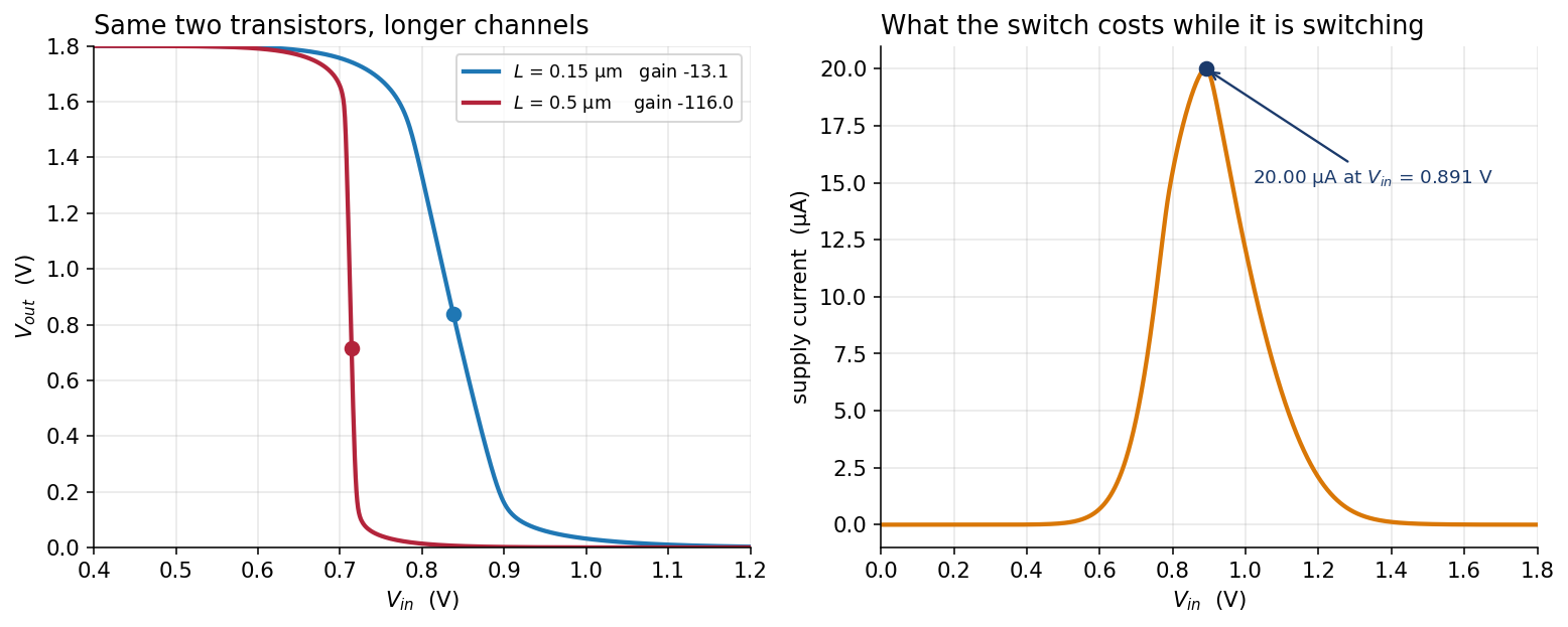
The minimum-length and long-channel inverters, and the supply current during a switch L = 0.15 um, Wn = Wp = 1 um gain -13.1253 at V_in = 0.814 V L = 0.5 um, Wn = Wp = 1 um gain -116.0341 at V_in = 0.712 V
You should see that the two device lines differ only in L, 0.15 against 0.5 (the rest of the diff is comments and the output file name). The long-channel inverter has 8.84× the voltage gain for 3.33× the channel length, from the same two transistors on the same supply.
Why does a longer channel give so much more gain, and which inverter would you use for which job?
Lab 04 measured the reason: \(r_o\) rises with \(L\), and the gain is \((g_{mn}+g_{mp})(r_{on} \parallel r_{op})\). A logic gate needs only enough gain to restore a degraded signal, and more than that doesn’t help it, whereas an amplifier wants every decibel it can get. So the same two transistors do a different job depending on \(L\): the minimum-length inverter is the logic gate, and the long-channel one is the amplifier.
Part 7: The current while it switches
How much supply current does an inverter draw, and when?
Read block 6 of
make extract, the supply current of the \(W_n = W_p\) = 1 µm inverter across its input sweep:supply current at V_in = 0 V 0.000002 uA supply current at V_in = 1.8 V 0.000320 uA peak supply current 20.0048 uA at V_in = 0.891 V
You should see almost nothing at either end and 20.0048 µA at \(V_{in}\) = 0.891 V.
Why is the current almost zero at both ends and largest near the middle, and what does that mean for power?
At either end of the sweep one of the two devices is off, so there is no path from vdd to ground. Near the middle both are on at once, and current runs straight from vdd to ground without doing any useful work. A CMOS gate therefore draws almost nothing while it holds a level and draws its current while it switches. That is why CMOS replaced everything before it, and why a processor gets hot when it computes and stays cool when it idles.
Part 8: The PMOS source on the wrong node
What happens when the PMOS source and body go to the wrong node?
Predict: will ngspice or the checker warn you about a PMOS whose source is on ground? Write down your guess.
Run the broken deck:
make brokenIt is
spice/vtc.spicewith one node name changed: the PMOS source and body go to0instead ofvdd.The sweep ran. 1801 rows, no errors, no warnings. Here is what it says the output does: V_in V_out supply current 0.000 V 0.000000000 V -0.000000 uA 0.300 V 0.000000000 V -0.000000 uA 0.600 V 0.000000000 V -0.000000 uA 0.900 V 0.000000000 V -0.000000 uA 1.200 V 0.000000000 V -0.000000 uA 1.500 V 0.000000000 V -0.000000 uA 1.800 V 0.000000000 V -0.000000 uA this curve never gets steeper than -1. Its steepest slope is -4.794e-15, which means the output barely responds to the input at all. A circuit with no gain above 1 cannot restore a logic level, so it is not a usable inverter whatever else it is. FAIL this circuit is not an inverterFind the change:
diff spice/vtc.spice spice/vtc_broken.spice. Apart from comments, spacing and the output file name, the only change is on theXPline, wherevdd vddbecame0 0.
You should see an output pinned at exactly zero for all 1801 points, a supply that delivers nothing, and no complaint from ngspice. ngspice has nothing to complain about, because the netlist is perfectly valid; a PMOS with its source on ground just can’t pull the output up. The check that catches this in one line, on any inverter, is the one the checker runs before anything else:
V_out(0.0 V) = 1.800000 V V_out(1.8 V) = 2.129252e-07 VRead both rails first. If the output doesn’t swing from one supply to the other, nothing else in the measurement means anything, and no amount of staring at \(V_M\) will tell you why.
Part 9: The current mirror
How accurately does a mirror copy a current, and what limits it?
Force 50 µA into a diode-connected reference and copy it four ways:
make mirror== spice/mirror.spice a 50 uA reference, copied four ways --- part 1: the reference branch sets a gate voltage --- v(ng) = 8.672678e-01 @m.xmref.msky130_fd_pr__nfet_01v8[vdsat] = 2.336319e-01 --- part 2: one gate voltage, three widths, V_out = 0.9 V --- i(vo2) = -5.00878e-05 i(vo3) = -1.12313e-04 i(vo4) = -2.39347e-04 and why the ratio is not what you drew: @m.xmw1.msky130_fd_pr__nfet_01v8[vth] = 5.894596e-01 @m.xmw2.msky130_fd_pr__nfet_01v8[vth] = 5.766246e-01 @m.xmw1.msky130_fd_pr__nfet_01v8[gm] = 3.340839e-04 @m.xmw2.msky130_fd_pr__nfet_01v8[gm] = 7.187672e-04 --- part 4: one W=10 device vs two W=5 devices in parallel --- i(vo3) = -1.12313e-04 i(vo5) = -1.00176e-04 --- part 3: the same 1:1 copy at several output voltages --- V_out = 0.1 V i(vo1) = -2.84076e-05 ... V_out = 1.8 V i(vo1) = -5.20797e-05Work out the 1:1 copy’s error at \(V_{out}\) = 0.9 V, from
i(vo2).In the
part 3block (it comes afterpart 4in the output), find the output voltage below which the copy collapses, and compare it with the reference branch’svdsat.Work out the actual ratios for the 2× and 4× outputs (
i(vo3)andi(vo4)againsti(vo2)), and the threshold difference between the 5 µm and 10 µm devices.Compare one W = 10 µm device (
i(vo3)inpart 4) with two W = 5 µm devices in parallel (i(vo5)), against twice the 1:1 current.
You should see a 1:1 copy good to 0.176 %, a collapse below about 0.2336 V, ratios of 2.2423 and 4.7785 instead of 2 and 4, a threshold 12.835 mV lower for the wide device, and the two parallel unit devices within 0.0004 % of twice the unit current.
Why does one wide device copy a current less accurately than two unit devices, and why does the copy collapse below 0.2336 V?
The wide device’s threshold is 12.835 mV lower, so at the same gate voltage it carries more current than its width alone would give. The two unit devices, on the other hand, are each the same 5 µm device as the reference, so together they carry twice its current. Below about 0.2336 V, which is the reference branch’s vdsat, the output device leaves saturation. The current mirror works through each of these.
Finishing
You’re done when make mine passes with your own xschem/my_inverter.sch and reports a switching threshold of 0.838029 V (Part 2).
Questions
- Why does the \(W_n = W_p\) inverter switch below \(V_{DD}/2\)? (Part 3.)
- Which \(W_p\) gives equal delays, which centres \(V_M\), and why are they different? (Part 5.)
- Why does one wide device copy a current less accurately than two unit devices? (Part 9.)
Submit
Nothing to submit. Keep xschem/my_inverter.sch, because AD104 starts from it.
Going further
Extensions
There are three, with reference answers in solutions/:
Why the foundry’s inverter isn’t symmetric.
sky130_fd_sc_hd__inv_1, the inverter LibreLane puts in your digital designs, has \(W_n\) = 0.65 µm and \(W_p\) = 1.0 µm, a ratio of 1.54, which is neither of this lab’s two answers. You can read the sizes yourself:grep -A3 'subckt sky130_fd_sc_hd__inv_1 ' \ /foss/pdks/sky130A/libs.ref/sky130_fd_sc_hd/spice/sky130_fd_sc_hd.spiceIt switches at 0.790872 V, 109 mV below centre, and that is deliberate. Work out why before you read the reference answer.
The delay arithmetic. Write out why equal drive currents give equal delays in Part 5, and check that the arithmetic closes.
More gain. Take
spice/vtc_long.spiceto longer \(L\) and find out how much gain two transistors can give.
SiliWiz
SiliWiz, which AD102 used to look at a resistor in cross-section, is worth one more visit: draw an NMOS in it, sweep the gate, and watch the channel you’ve been calculating about appear under the oxide.
Your inverter in AD104
You now have a schematic of a real logic gate, sized by you against a criterion you chose and verified against a simulation to five digits. AD104: Layout takes this file and asks you to draw it as geometry in Magic. Every transistor becomes a rectangle of diffusion under a stripe of poly, and every net becomes metal with a width and a spacing. Then Magic runs DRC to check that a fab could make what you drew, and netgen runs LVS to show that what you drew is the same circuit as your schematic, node for node and device for device.
This is the foundry’s own inverter, sky130_fd_sc_hd__inv_1, opened in Magic:
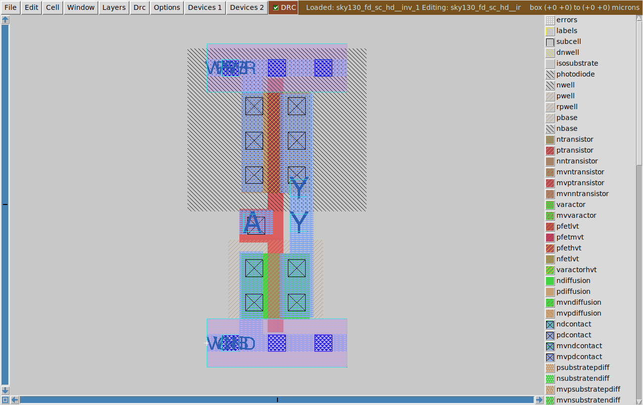
Every hatch pattern in that window is a mask layer, listed by name on the right. A enters on local interconnect, crosses both channels as the single poly stripe in the middle, and Y leaves on local interconnect. These are the nets on your schematic: A is in, Y is out, and the VPWR and VGND rails along the top and bottom are vdd and 0, all drawn here as rectangles.
The geometry has to obey design rules, and Magic checks them continuously while you paint. If you drop a metal1 shape 0.04 µm from the power rail, Magic tells you before you’ve even finished the wire:
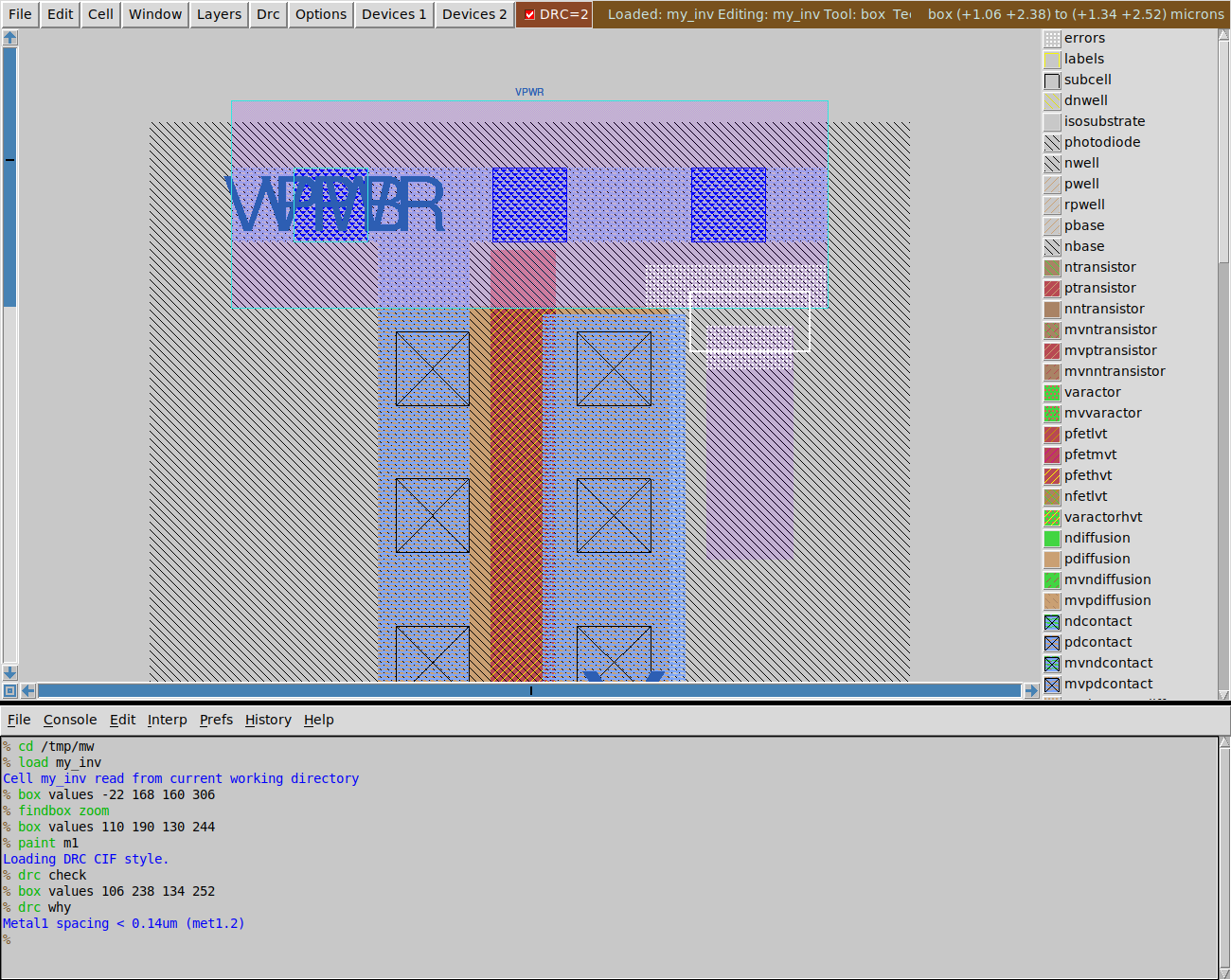
drc why in the console printing “Metal1 spacing < 0.14um (met1.2)”The white hatch is the error region, DRC=2 in the toolbar counts errors live as you edit, and drc why names the rule that was broken: Metal1 spacing < 0.14um (met1.2).
Three things from AD103 come back in AD104:
- \(W\) and \(L\) are geometry. In Magic you draw them with a mouse instead of typing them, so the
W=1versusW=1utrap disappears, because there’s no number to put a unit on. nf=2, the multi-finger device from Lab 04 that changed the current by 4.5 % with no change to \(W\) or \(L\), becomes a picture: two gate stripes sharing a drain.- Unit devices in an array, from the current mirror. AD104 is where you see what a mirror looks like when it is drawn properly, dummies and all.
Stuck, or want to argue about any of this? Ask in the team Discord, and bring the number you got and the number you expected.
Next on the Course path: you’ve finished AD103. The next course is AD104: Layout, and it starts from your xschem/my_inverter.sch.