Lab 04: Testing the W/L rule
The square law says that only the ratio \(W/L\) matters:
\[ I_D^{\text{sat}} = \tfrac12\,\mu_n C_{ox}\frac{W}{L}\,(V_{GS}-V_{TH})^2 \]
You’ll test that claim on seventeen transistors at one bias point, after first writing down your own predictions for six of them. The rule gets two of those six right to within 3 % and misses the other four by up to 91 %, and the signs of those errors follow a pattern you can read straight off the scoring table. Five of the devices have a \(W/L\) of exactly 5, and they carry five different currents. Between writing the predictions and scoring them, you’ll use the Lab 03 package to watch the threshold move and to measure how much gain one transistor can give.
Package: labs/lab-04-wl-knob/, plus three targets in labs/lab-03-mosfet-regions/
Before you start
- Finish Lab 03. This lab uses its reference device, \(W\) = 5 µm, \(L\) = 1 µm at 696.2755 µA, as the anchor for every prediction.
- Read What moves the threshold, Transconductance and output resistance and Sizing with W and L.
- Open a terminal in the workbench. Both
Makefiles setPDK=sky130Athemselves, so no other setup is needed.
Time: about 2 hours. make in this lab takes about 40 seconds; each Lab 03 target in Parts 2 and 3 takes about ten. Those wall times depend on your machine, but every other number on this page is fixed, and the checker enforces it.
Part 1: Write your predictions
What does the \(W/L\) rule predict for six devices? Do this before you run anything. It takes ninety seconds, and it’s the only part of the lab you can’t redo afterwards, because once you’ve seen the measured currents you can’t predict them honestly any more.
Go to the lab folder, then open
predictions.txtin a text editor:cd /foss/designs/modules/ad103/labs/lab-04-wl-knobRead the header. Your one measured anchor is the Lab 03 device: W = 5 µm, L = 1 µm, \(V_{GS} = V_{DS}\) = 1.8 V, \(I_D\) = 696.2755 µA.
For each of the six devices, write the current the \(W/L\) rule predicts, in microamps, to one decimal place, after the
=. Write only the number, becausemake predictdoesn’t read a line that ends inuA. Don’t run anything first, and don’t go back and change a prediction once you’ve seen the answer.P1 W=10 L=1 = P2 W=50 L=1 = P3 W=5 L=2 = P4 W=5 L=0.15 = P5 W=0.75 L=0.15 = P6 W=20 L=4 =Save the file.
You should see six numbers in predictions.txt. Leave the file alone until Part 4, where you score them.
Part 2: Move the threshold
How far do body bias, temperature and channel length move \(V_{TH}\)? The two decks that answer this are in the Lab 03 package.
Go to the Lab 03 folder and lift the source above the bulk:
cd ../lab-03-mosfet-regions
make vth-body
== spice/vth_body.spice --- vth and I_D vs V_SB, W = 5 um, L = 1 um, V_GS = 1.8 V, V_DS = 0.05 V --- V_SB = 0 V @m.xm1.msky130_fd_pr__nfet_01v8[vth] = 5.894596e-01 i(vds) = -6.63374e-05 ... V_SB = 1.2 V @m.xm1.msky130_fd_pr__nfet_01v8[vth] = 8.222507e-01 i(vds) = -5.15967e-05 --- and the same device, V_SB = 0, at three temperatures --- T = -40 C @m.xm1.msky130_fd_pr__nfet_01v8[vth] = 6.499250e-01 i(vds) = -9.38168e-05 ... T = 125 C @m.xm1.msky130_fd_pr__nfet_01v8[vth] = 5.010177e-01 i(vds) = -4.50650e-05The rows marked
...here, the 27 °C row among them, are printed in full in your terminal, and they’re also tabulated on What moves the threshold.Work out the threshold shift at each \(V_{SB}\), relative to \(V_{SB}\) = 0, and the drop in drain current at \(V_{SB}\) = 1.2 V. Check one row against the body-effect formula with \(\gamma\) = 0.4108 √V and \(2\phi_F\) = 0.600 V.
From the temperature block, work out the threshold’s slope in mV/°C, and the change in current from 27 °C to 125 °C. Predict the sign of the current change before you calculate it.
Measure the threshold at nine channel lengths:
make vth-l== spice/vth_vs_l.spice L model vth 0.15 um 7.078517e-01 V 0.2 um 6.872240e-01 V 0.3 um 6.553824e-01 V 0.5 um 6.300670e-01 V 0.8 um 6.003750e-01 V 1 um 5.894596e-01 V 1.5 um 5.627056e-01 V 2 um 5.495175e-01 V 4 um 5.364102e-01 V
You should see a threshold shift of +232.791 mV at \(V_{SB}\) = 1.2 V, with 22.2 % less current, and the body-effect formula should agree with the measurement to within a fraction of a millivolt. The threshold’s temperature slope is about −0.9 mV/°C, and the hot device carries 32.1 % less current than the one at 27 °C. As the length shrinks from 4 µm to 0.15 µm, the threshold rises by 171.44 mV. What moves the threshold explains each of these.
Part 3: Efficiency and intrinsic gain
How much voltage gain can one transistor give, and how does that depend on \(L\)?
Predict: as \(L\) goes from 0.15 µm to 4 µm, does \(g_m r_o\) rise or fall? Write it down.
Still in the Lab 03 folder, measure \(g_m\) and \(g_{ds}\) at four lengths and six gate voltages:
make gm-roThe first block covers four lengths at \(V_{GS} = V_{DS}\) = 1.8 V, and the first of them reads:
--- W = 5 um, V_GS = V_DS = 1.8 V, four channel lengths ---
L = 0.15 um
i(vda) = -2.64419e-03
@m.xma.msky130_fd_pr__nfet_01v8[gm] = 2.468806e-03
@m.xma.msky130_fd_pr__nfet_01v8[gds] = 2.787163e-04
The second block steps the gate of the L = 1 µm device from 0.7 V to 1.8 V.
For each length, compute \(r_o = 1/g_{ds}\) and the intrinsic gain \(g_m r_o = g_m/g_{ds}\).
In the second block, compute \(g_m/I_D\) at \(V_{GS}\) = 0.7 V and at 1.8 V. Compare both with the ceiling of 26.9 /V from Transconductance and output resistance.
You should see an intrinsic gain of 8.86 at L = 0.15 µm rising to 106.11 at L = 4 µm, even though \(g_m\) falls by a factor of nine over the same range. In the second block, \(g_m/I_D\) is 13.50 /V at \(V_{GS}\) = 0.7 V, about half the ceiling, against only 1.31 /V with the gate wide open.
Part 4: Run the lab and score your predictions
Which of your six predictions land, and is there a pattern in the misses?
Go back to the Lab 04 folder and run the four decks:
cd ../lab-04-wl-knob
make
== spice/w_ladder.spice wrote results/w_ladder.log == spice/l_ladder.spice wrote results/l_ladder.log == spice/same_ratio.spice wrote results/same_ratio.log == spice/double_w.spice wrote results/double_w.log == checking YOUR NUMBERS ok I_D W=1 L=1 127.1470 uA (reference 127.1470) ok I_D W=5 L=1 696.2755 uA (reference 696.2755) ok I_D W=10 L=1 1395.3200 uA (reference 1395.3200) ok I_D W=50 L=1 6762.1370 uA (reference 6762.1370) ok I_D W=5 L=0.15 2644.1910 uA (reference 2644.1910) ok I_D W=5 L=4 197.9738 uA (reference 197.9738) ok I_D W=0.75 L=0.15 364.9284 uA (reference 364.9284) ok I_D W=20 L=4 798.0193 uA (reference 798.0193) ok two W=5 in parallel 1392.5510 uA (reference 1392.5510) ok vth(W=10) - vth(W=5) -12.8354 mV (reference -12.8354) 2 x I_D(W=5) = 1392.5510 uA two W=5 in parallel = 1392.5510 uA (difference +0.000000 uA) PASS all ten measured values match the reference runEvery run also leaves a three-line
bsim4v5.outin the lab folder. It’s harmless, and Eta0 is negative on the ngspice survival card has the details.Score your predictions:
make predictdevice W/L the W/L rule measured rule err your guess your err ------------------------------------------------------------------------------------------------ W=10 L=1 10.00 1392.551 uA 1395.3200 uA -0.2 % -- -- W=50 L=1 50.00 6962.755 uA 6762.1370 uA +3.0 % -- -- W=5 L=2 2.50 348.138 uA 380.7284 uA -8.6 % -- -- W=5 L=0.15 33.33 4641.837 uA 2644.1910 uA +75.5 % -- -- W=0.75 L=0.15 5.00 696.275 uA 364.9284 uA +90.8 % -- -- W=20 L=4 5.00 696.275 uA 798.0193 uA -12.7 % -- --The sample above was made with an empty
predictions.txt, which is why its last two columns are--. With your file filled in, your own numbers appear there instead. (Ifmake predictsayspredictions.txt still has 6 blank(s), you didn’t save the file in Part 1.)Cover the last two columns and read only
rule err, top to bottom. Each entry is the rule’s error as a percentage of the measured current. That’s why the L = 2 µm row reads −8.6 % here, while Sizing with W and L calls the same gap 9.4 % more current than \(1/L\) predicts: that page takes it as a percentage of the rule’s 348.138 µA.
You should see your six predictions in the your guess column. In rule err, the two rows where only \(W\) changed are within 3 %, and the four where \(L\) changed are out by 8 to 91 %. That error is positive every time \(L\) got shorter and negative every time it got longer.
Which half of \(W/L\) can you use in a hand calculation, and which half can’t you?
You can use \(W\), because changing it on its own kept the rule within 3 %. \(L\) is the half you can’t trust: the rule over-predicts the current of every shorter device and under-predicts every longer one, by 8 to 91 %.
Part 5: Width
Is current proportional to \(W\), and is “twice as wide” the same as “two of them”?
Print every table this lab produces, with its working:
make extractRead block 1, the W ladder, and open
results/ad103-w-ladder.png: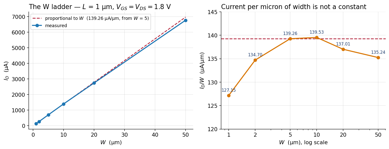
The W ladder: measured current against the proportional-to-W line, and current per micron of width W (um) I_D I_D / W W x I(W=1) model vth 1 127.1470 uA 127.1470 uA/um +0.00 % 615.2253 mV 2 269.4032 uA 134.7016 uA/um -5.61 % 603.4546 mV 5 696.2755 uA 139.2551 uA/um -8.69 % 589.4596 mV 10 1395.3200 uA 139.5320 uA/um -8.88 % 576.6242 mV 20 2740.1490 uA 137.0075 uA/um -7.20 % 564.0813 mV 50 6762.1370 uA 135.2427 uA/um -5.99 % 556.5815 mVOn the left plot, the measurement and the proportional-to-\(W\) line lie almost on top of each other, so the difference is hard to see there. Look at the right plot instead, which shows the same data divided by \(W\).
Read block 2, six ways of asking for “twice as wide”:
   A   W=5            696.2755 uA   1.0000 x A   the reference
   B   W=10          1395.3200 uA   2.0040 x A   drawn twice as wide
   C   W=5 + W=5     1392.5510 uA   2.0000 x A   two of A, wired in parallel
   D   W=5 m=2       1392.5510 uA   2.0000 x A   ngspice's own multiplier
   E   W=5 mult=2     696.2755 uA   1.0000 x A   the subckt's 'multiplier'
   F   W=10 nf=2     1458.1360 uA   2.0942 x A   folded into two fingers

   A doubled by hand    1392.5510 uA
Compare C and D with the last line, digit by digit.
You should see current per micron of width climb 9.7 % from \(W\) = 1 to \(W\) = 10 and then fall 3.1 % by \(W\) = 50, while the model’s vth falls at every step of the ladder, by 58.6438 mV in all. In block 2, C and D both match the hand-doubled 1392.5510 to every digit, so two 5 µm transistors in parallel carry exactly twice the current of one, and so does m=2.
Over this hundredfold range of width, is “current is proportional to \(W\)” good enough to use? And can the falling vth explain both the rise and the fall in current per micron?
Yes, you can use it, because it’s wrong by less than 10 % over the whole ladder. The direction of the vth trend makes sense (a wider device has a lower threshold, so it turns on harder), but a cause that only ever moves one way can’t on its own produce a rise and then a fall. Something else must push the other way beyond \(W\) = 10 µm, and this course doesn’t claim to know what it is.
Now work out what each of the other rows in block 2 says.
B is 2.0040× A rather than 2.0000×. Why isn’t one 10 µm device the same as two 5 µm ones?
TipAnswerOne 10 µm device carries 2.7690 µA (+0.199 %) more than two 5 µm ones. The model reports
vth= 589.4596 mV for the 5 µm device and 576.6242 mV for the 10 µm one, 12.8354 mV apart even though the bias and length are identical. So width enters the model itself rather than only multiplying its result, and that makes “twice as wide” and “two of them” different circuits.E says
mult=2and carries exactly what A does. Why?TipAnswerThe SKY130 subcircuit declares a parameter called
multand never uses it. You can see this in/foss/pdks/sky130A/libs.ref/sky130_fd_pr/spice/sky130_fd_pr__nfet_01v8__tt.pm3.spice, where the.subckt’s.paramline listsmult = 1and the device line inside carries nom = {mult}. So if you writemult=2in a deck by hand, it’s accepted and ignored, and nothing tells you so;m=2is the parameter that works. XSchem’s symbol writesm=for you whenevermultisn’t 1. If you setmult=2in the property editor, the device line comes out... sd=0 mult=2 m=2, and the current doubles. (Atmult=1the line ends... sd=0 mult=1with nom=, because there is nothing to multiply.) That’s why drawing the schematic gets this right, and copying a device line by hand doesn’t.F has the same \(W\), \(L\) and bias as B, and 4.50 % more current. What is different?
TipAnswernf=2folds one 10 µm channel into two 5 µm fingers that share a drain diffusion. Nothing in \(W/L\) describes that, because it’s a fact about the layout, and you’ll draw it in AD104.
Don’t push
nfhigher to see how far the effect goes.W=10 nf=5aborts the entire run withFatal: Drout = -1.76308 is negativeanddoAnalyses: no such parameter on this device or parameter is missing. That is a BSIM parameter check failing inside one of the model bins, not a mistake you made, and two fingers are enough to show the effect.
Part 6: Length
How badly does \(1/L\) fail, and why?
Read block 3 of
make extract, the L ladder, and openresults/ad103-l-ladder.png: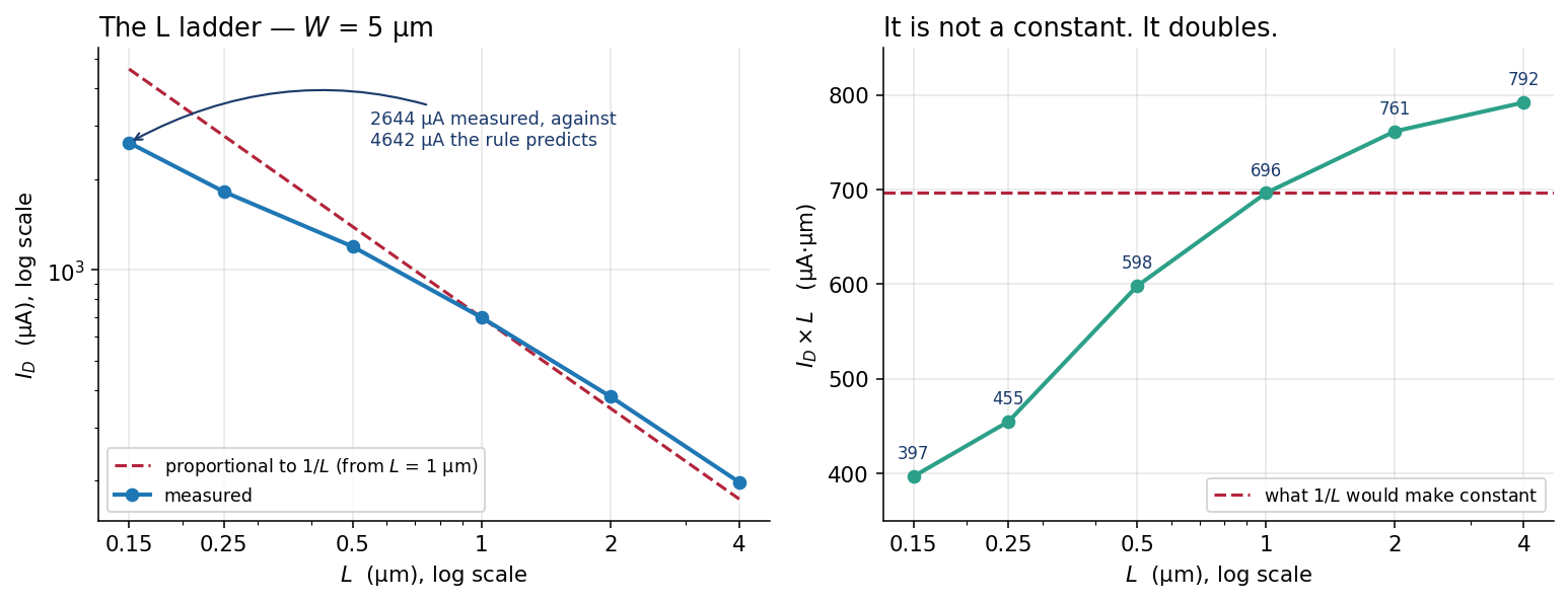
The L ladder on log axes, and I_D times L, which 1/L says should be constant L (um) I_D I_D x L vs 1/L from L=1 vth vdsat 0.15 2644.1910 uA 396.6287 +75.55 % 707.44 351.92 mV 0.25 1818.6050 uA 454.6513 +53.14 % 658.63 426.29 mV 0.5 1196.0170 uA 598.0085 +16.43 % 626.23 628.45 mV 1 696.2755 uA 696.2755 +0.00 % 589.46 779.46 mV 2 380.7284 uA 761.4568 -8.56 % 549.52 912.45 mV 4 197.9738 uA 791.8952 -12.07 % 536.41 1001.27 mVThe \(I_D \times L\) column is the one that tests the rule: if current really went as \(1/L\), that column would show the same number in all six rows.
Compare
vdsatwith the overdrive \(V_{GS} - V_{TH}\) for the shortest and longest devices (1092.6 mV and 1263.6 mV).Read the end of the block, which closes the gap at L = 0.15 µm one effect at a time:
   Closing the L = 0.15 um gap, one effect at a time:
     1/L alone                                   4641.837 uA
     1/L, with each device's own vth and (V_ov)^2  3781.114 uA
     measured                                    2644.191 uA
   The threshold step closes 43.1 % of the gap.
You should see \(I_D \times L\) run from 396.63 to 791.90, so it doubles across the ladder, and vdsat run from 351.92 mV to 1001.27 mV. Correcting for each device’s threshold closes less than half of the gap at 0.15 µm.
The 0.15 µm device stopped responding to its drain at a third of the overdrive the square law assumed. What does that tell you, and why can’t more arithmetic on vth close the rest of the gap?
It tells you the device is velocity saturated, and that’s why \(1/L\) over-promises on every short device. No further arithmetic on vth can close the rest of the gap, because the square law has no term for a carrier speed limit. At this point hand calculation runs out, and you need the simulator.
Part 7: Five devices with \(W/L\) = 5
Five devices share a \(W/L\) of 5 but differ in area. What does the extra area buy?
Read block 4 of
make extract, and openresults/ad103-same-ratio.png: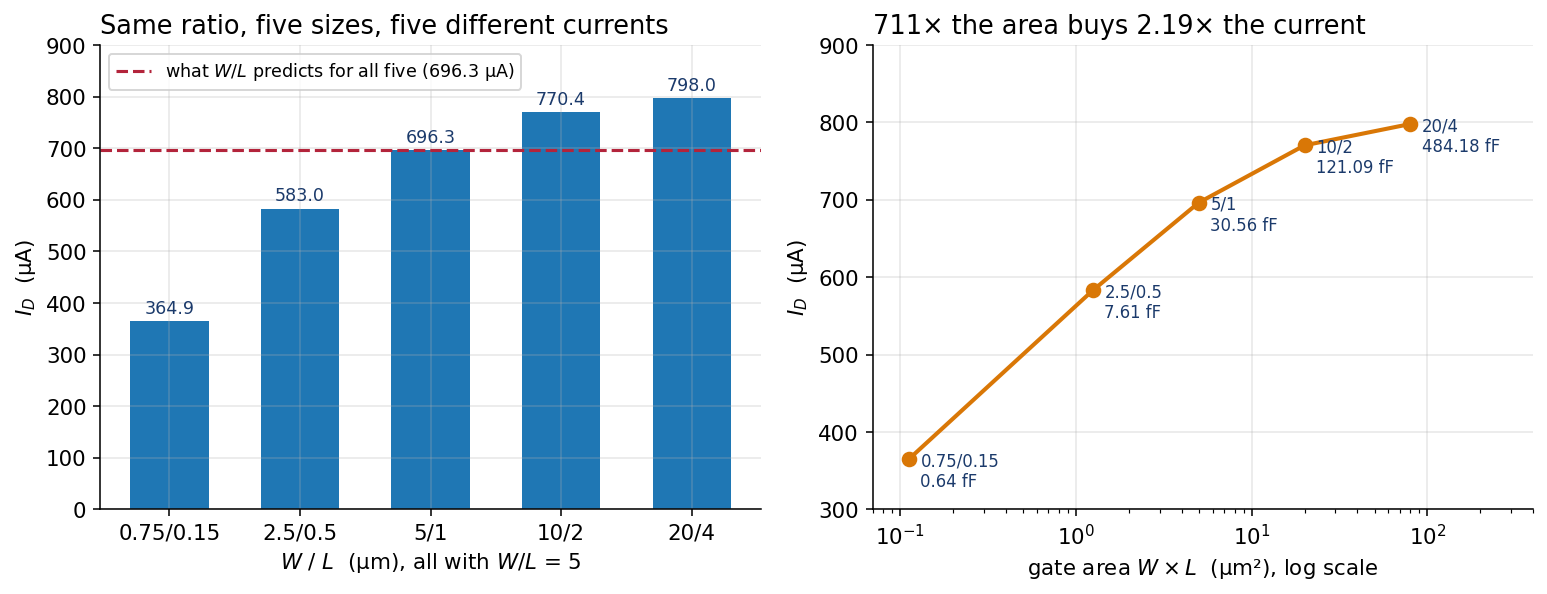
Five devices with W/L = 5, and what their area buys W / L I_D gate area cgg I_D per um^2 0.75 / 0.15 364.9284 uA 0.1125 um^2 0.6427 fF 3243.81 uA/um^2 2.5 / 0.5 582.9524 uA 1.2500 um^2 7.6137 fF 466.36 uA/um^2 5 / 1 696.2755 uA 5.0000 um^2 30.5632 fF 139.26 uA/um^2 10 / 2 770.4110 uA 20.0000 um^2 121.0871 fF 38.52 uA/um^2 20 / 4 798.0193 uA 80.0000 um^2 484.1798 fF 9.98 uA/um^2Check the ratio in the first column: 0.75/0.15 = 5, 20/4 = 5, and so is every row in between.
Work out what the largest device buys over the smallest: the ratio of currents, of gate areas and of gate capacitances.
Read the two
gdslines at the end of the block:gds(0.75/0.15) = 38.855 uS -> r_o = 25.74 kohm gds(20/4) = 7.435 uS -> r_o = 134.50 kohm
You should see currents from 364.9284 µA to 798.0193 µA, a factor of 2.1868, for identical \(W/L\) at identical bias. The biggest device gets 2.19× the current of the smallest for 711× the gate area and 753× the gate capacitance, so per square micron of gate the small one is 325× more efficient. The biggest device’s output resistance is 5.23× the small one’s.
What does the biggest device buy for its 711× area?
It doesn’t buy much current: 2.19× for 711× the area. Area costs money, and gate capacitance costs time, because whatever drives the gate has to charge it. What the area does buy is 5.23× the output resistance. An amplifier’s gain is \(g_m r_o\), so that factor is the reason an analog designer pays for a long channel, and the reason a digital designer doesn’t.
Part 8: Read a FAIL you caused
What does the checker tell you when one number is 3 % off?
Hand the checker a run that is 3 % wrong:
make brokenIt copies your W ladder, moves the \(W\) = 10 µm current by 3 %, and hands the result to the checker. A 3 % error is far too small to see by eye, but it’s large enough to mean you simulated the wrong device.
  XX  I_D  W=10 L=1                 1437.1800 uA  (reference 1395.3200)
...
FAIL
  - I_D  W=10 L=1: got 1437.1800, reference 1395.3200 (+3.00 %)

  Three things cause this, in order of how often:
   1. A unit suffix on W or L somewhere in spice/. They are plain
      microns. Check with:  grep -n 'W=[0-9.]*[a-z]' spice/*.spice
Run
makeagain to get back toPASS.
You should see one XX row among nine ok rows. The FAIL section names the number and gives both values and the percentage, then lists three causes in order of how often they happen, with a grep for the first one.
Finishing
You’re done when make predict shows your six predictions in the your guess column, next to the measurements, with your own errors in your err (Part 4).
Questions
- Which half of \(W/L\) can you trust in a hand calculation, and by roughly how much? (Part 4.)
- Why does one 10 µm device differ from two 5 µm devices in parallel? (Part 5, row B.)
- Five devices with \(W/L\) = 5: what does the largest one buy for its 711× area? (Part 7.)
Submit
Nothing to submit.
Going further
Three extensions, with reference answers in solutions/. For each one, predict first, then run it, and only then read the answer.
- Widen further. Add
W=100to the W ladder, thenW=200. One of them tells you where the model ends, and the error it gives is one you have already met for a completely different reason. - Repeat the ladder in PMOS. Build the same ladder out of
pfet_01v8. At \(L\) = 1 µm the NMOS carries 6.685× the PMOS; the capstone measures the same ratio at \(L\) = 0.15 µm and gets 2.496, so the ratio between the two device types isn’t a property of the process alone. - Lower the gate. Re-run the L ladder at \(V_{GS}\) = 0.9 V. If velocity saturation is really what breaks \(1/L\), the short-channel error should shrink at the lower gate voltage, and it does, from +75.5 % to +29.5 %. Then look at what happens at the long end.
Next on the Course path: read The CMOS inverter.